Method and Device for Cadmium-Free Solar Cells

a technology of solar cells and cadmium, applied in the field of photovoltaic materials and manufacturing methods, can solve the problems of low energy conversion efficiency of devices made from such crystalline materials, many limitations remain to be resolved, and high cost of crystalline materials, so as to save processing materials, reduce environmental harm, and high photovoltaic efficiency

Inactive Publication Date: 2012-09-27
CM MFG
View PDF26 Cites 30 Cited by
  • Summary
  • Abstract
  • Description
  • Claims
  • Application Information

AI Technical Summary

Benefits of technology

[0009]Many benefits can be achieved by embodiments according to the present invention. For example, the thin film single junction photovoltaic cell can be fabricated using in a simplified process, yet with conventional equipment. Advantages of the embodiments of the present method eliminate the use of toxic elements such as cadmium. The process further saves processing material and reduces environmental harm, yet the device achieves high photovoltaic efficiency without need of a buffer layer. The device and its manufacturing method lead to a much improved cost saving and cleaner way to convert sunlight into electric energy.

Problems solved by technology

Although solar energy is environmentally clean and has been successful to a point, many limitations remain to be resolved before it becomes widely used throughout the world.
However, crystalline materials are often costly and difficult to make on a large scale.
Additionally, devices made from such crystalline materials often have low energy conversion efficiencies.
Similar limitations exist with the use of thin film technology in making solar cells.
That is, efficiencies are often poor.
Additionally, thin-film photovoltaic cells traditionally use exotic elements including cadmium, mercury, or telluride, which substantially limit the applications and cause environmental side effects.
Often, such thin-film solar devices are difficult to handle during their manufacture processes because of these toxic materials.

Method used


Image

  • Method and Device for Cadmium-Free Solar Cells
  • Method and Device for Cadmium-Free Solar Cells
  • Method and Device for Cadmium-Free Solar Cells

Examples


Embodiment Construction

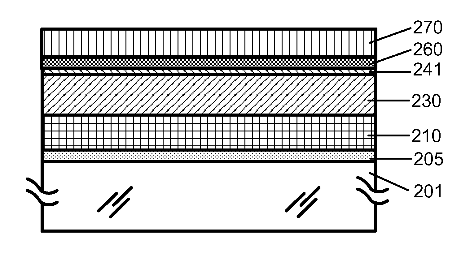
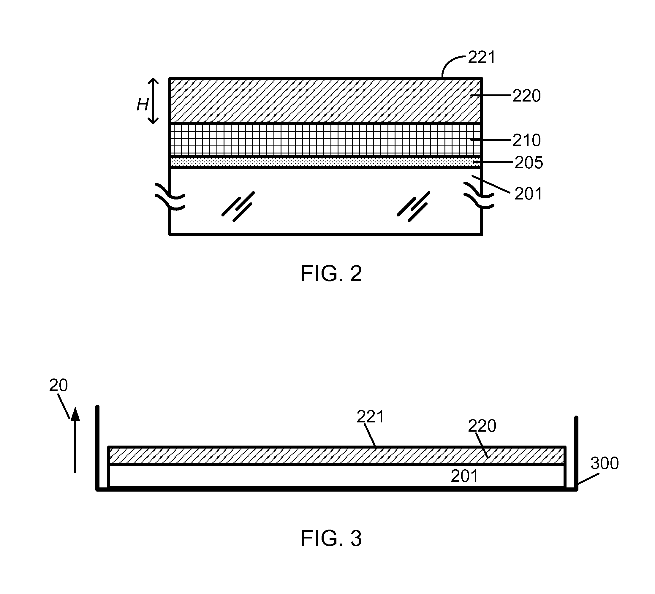
[0017]FIG. 1 is a process flow diagram illustrating a method of fabricating a thin film photovoltaic device. As shown, the method 100 begins with a process 110 for providing a substrate for fabricating a thin-film photovoltaic device. The resulting device is illustrated in FIG. 2. In the example, substrate 201 is a transparent material such as glass, fused silica, or quartz. In a specific embodiment, the substrate is a soda lime glass. The process 110 includes forming a barrier material 205 overlying the substrate 201. The barrier material is used as a diffusion barrier for preventing sodium and other elements in the soda lime glass substrate from diffusing into the solar cell. Barrier material 205 can be silicon oxide, silicon nitride, titanium nitride, or other material. The process 110 further includes forming a conductive material 210 overlying the barrier material 205. In an example, the conductive material 210 can be patterned across the substrate to form a plurality of cell s...


PUM

PropertyMeasurementUnit
distanceaaaaaaaaaa
distanceaaaaaaaaaa
temperatureaaaaaaaaaa

Abstract

A method for fabricating a thin film photovoltaic device is provided. The method includes providing a substrate comprising a thin film photovoltaic absorber which has a surface including copper, indium, gallium, selenium, and sulfur. The method further includes subjecting the surface to a material containing at least a zinc species substantially free of any cadmium. The surface is heated to cause formation of a zinc doped material. The zinc doped material is free from cadmium. Furthermore the method includes forming a zinc oxide material overlying the zinc doped material and forming a transparent conductive material overlying the zinc oxide material.

Description

CROSS-REFERENCE TO RELATED APPLICATION[0001]This application claims priority to U.S. Provisional Application No. 61 / 389,129, entitled “Method and Device for Cadmium-Free Solar Cells,” filed on Oct. 1, 2010, by Kannan Ramanathan and Robert D. Wieting, commonly assigned, and hereby incorporated by reference in its entirety herein for all purpose.BACKGROUND OF THE INVENTION[0002]The present invention relates generally to photovoltaic materials and manufacturing method. More particularly, the invention provides a device for a thin-film photovoltaic cell without a cadmium-based buffer layer and a method for making thereof. The present method and device provide a thin film photovoltaic cell using a copper indium diselenide absorber material and a cadmium-free window buffer material.[0003]Environmentally clean and renewable sources of energy are desired. An example of a clean source of energy is hydroelectric power. Clean and renewable sources of energy also include wind, waves, biomass, a...

Claims


Application Information

Patent Timeline
Patent Type & Authority Applications(United States)
IPC IPC(8): H01L31/0749H01L31/18
CPCH01L31/0749H01L31/0322Y02E10/547H01L31/068Y02E10/541H01L31/0323H01L31/0682
Inventor RAMANATHAN, KANNANWIETING, ROBERT D.
Owner CM MFG
Why Eureka
Try Eureka