

Plasma processing apparatus
a plasma processing apparatus and plasma technology, applied in liquid surface applicators, coatings, electric discharge tubes, etc., can solve the problems of insufficient study of passive antenna operation, inability to meet the diverse and high-degree of process performance required by a recent plasma processing apparatus, and inability to accurately control the plasma density distribution. , to suppress the wavelength
- Summary
- Abstract
- Description
- Claims
- Application Information
AI Technical Summary
Benefits of technology
Problems solved by technology
Method used
Image

Examples
example 1
[Example 1 of Configuration of Floating Coil]
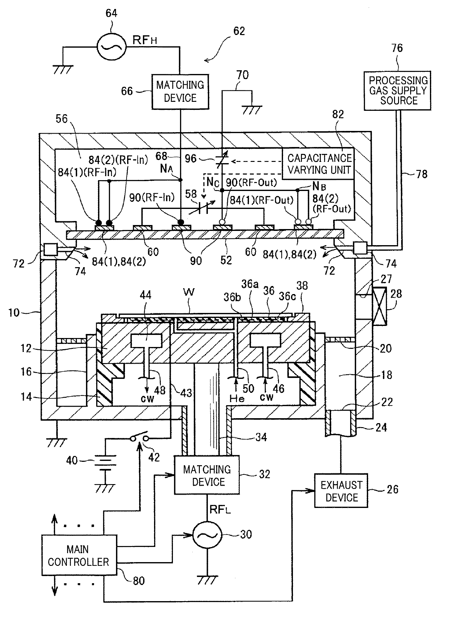
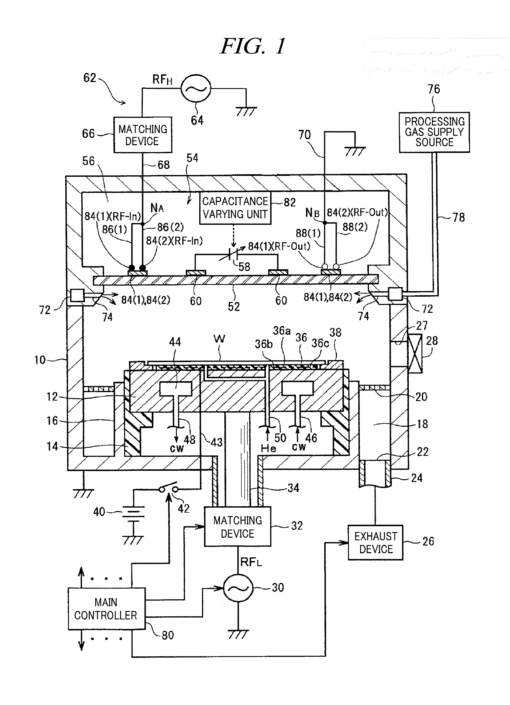
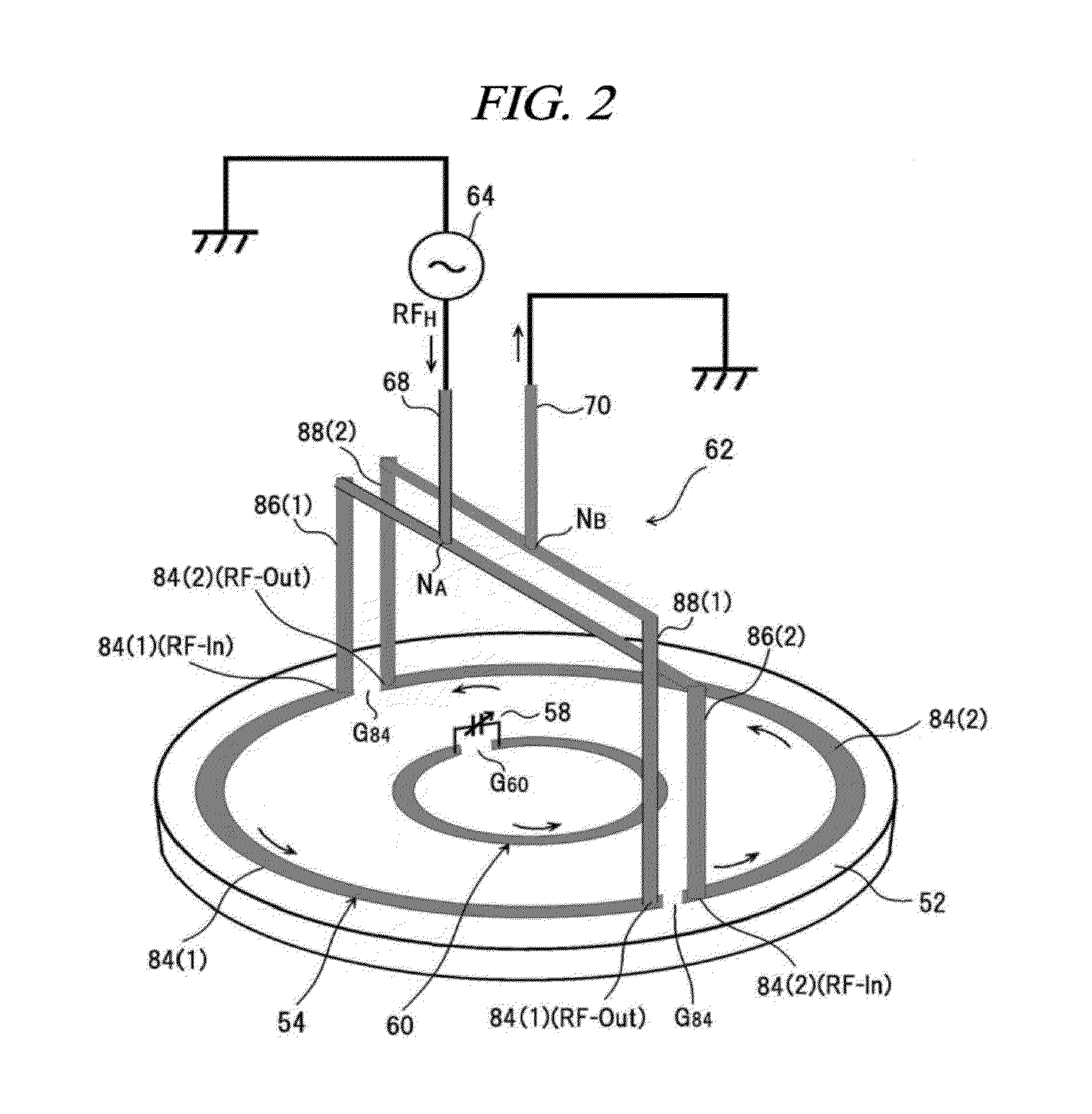
[0160]Hereinafter, when a commercially available capacitor is used as the variable capacitor 58, configuration examples of the variable capacitor 58 in the floating coil 60 of the inductively coupled plasma processing apparatus of the illustrative embodiments will be explained with reference to FIGS. 11 to 15.
[0161]In the example illustrated in FIG. 11, the gap G60 is formed at the floating coil 60, and a commercially available two-terminal capacitor 58 is provided at a position of the gap. In this example, capacitor connection conductors 100a and 100b that connect the coil conductor of the floating coil 60 with a terminal of a package main body of the capacitor 58 are stood uprightly from (desirably, uprightly above) the coil conductor.
[0162]As described above, when a high induced current IIND flows in the floating coil 60, a large-sized variable capacitor 58 that allows a high current to pass is used. However, as the size of the capacit...
example 2
[Example 2 of Configuration of Floating Coil]
[0173]Hereinafter, referring to FIGS. 16 to 18, there will be explained an example in which the variable capacitor 58 as a structure is provided at the floating coil 60 as a part thereof.
[0174]As depicted in FIG. 16, in this example, plate-shaped or sheet-shaped dielectric member 108 and fixed contact conductor 110 having the same thickness are fixed on a coil conductor end 60a adjacent to the gap G60. Herein, the fixed contact conductor 110 is positioned farther from the gap G60 than the dielectric member 108. A plate-shaped or sheet-shaped fixed contact conductor 112 having the same thickness is fixed on the other coil conductor end 60b adjacent to the gap G60 on the opposite side. A movable electrode 114 is configured to slidably move on upper surfaces of the fixed contact conductor 110, dielectric member 108, and fixed contact conductor 112 arranged in a plane so as to move along the circumferential direction. The circumferential dire...
modification example
Another Illustrative Embodiment or Modification Example
[0229]A loop shape of a coil of a RF antenna in accordance with the present illustrative embodiments is not limited to a circular shape. Although not illustrated, it may be a square shape or a triangular shape. Further, a multiple number of coil segments of each antenna coil (loop) may have a different shape and different self-impedance to one another.
[0230]In the present illustrative embodiments, an impedance control unit of the RF antenna is not limited to a fixed capacitor or a variable capacitor as described above. By way of example, it may be a coil or an inductor or a unit including a capacitor and an inductor and may also include a resistance component.
[0231]FIG. 47 illustrates a configuration example in which a transformer 160 is provided between the matching device 66 of the high frequency power supply unit 62 and the RF antenna 54. A first wound wire of the transformer 160 is electrically connected to the output termin...
PUM
| Property | Measurement | Unit |
|---|---|---|
| Length | aaaaa | aaaaa |
| Dielectric polarization enthalpy | aaaaa | aaaaa |
| Diameter | aaaaa | aaaaa |
Abstract
Description
Claims
Application Information