
Electronic component-embeded board and method for manufacturing the same

a technology of electronic components and embedded boards, which is applied in the field of electronic component embedded boards, can solve the problems of unfavorable performance enhancement of the whole device, slight lowering of the conductive characteristics of electronic components, and disadvantageous increase to deteriorate conductive characteristics, etc., and achieves excellent close contact properties, high electric resistance, and increase of the electric resistance in the connecting portion.

Active Publication Date: 2012-10-04
TDK CORPARATION
View PDF3 Cites 23 Cited by
  • Summary
  • Abstract
  • Description
  • Claims
  • Application Information

AI Technical Summary

Benefits of technology

[0008]Thus, the present invention has been developed in view of such situations, and an object thereof is to provide an electronic component-embedded board, which can effectively prevent damages of the electronic component, and the generation of a defect or the lowering of a yield due to the damages and which can simultaneously alleviate an electric resistance in a connecting portion between each of terminals of the electronic component and a wiring line to improve conductive characteristics and which can further enhance close contact properties between each IC terminal and a resin insulating layer, and to provide a method for manufacturing the electronic component-embedded board.
[0017]According to an electronic component-embedded board and a method for manufacturing the electronic component-embedded board of the present invention, a wiring layer is connected to a connection layer positioned on a lower layer side than the wiring layer and having a comparatively low electric resistance, via no outermost surface layer having a comparatively high electric resistance. Therefore, the increase of the electric resistance of the corresponding portion can be suppressed. Furthermore, when an opening is processed and formed in the insulating layer, the lower layer-side connection layer in each of terminals of an electronic component is protected by the outermost surface layer, and the damages of the connection layer are prevented. Moreover, when the outermost surface layer excellent in close contact properties with the insulating layer is employed, the close contact properties between each of the terminals (terminal portions) of the electronic component and the insulating layer can significantly be enhanced as compared with a configuration where the insulating layer is bonded to the connection layer. In consequence, it is possible to effectively prevent the generation of a defect of the electronic component-embedded board or the lowering of a yield due to the peeling of the electronic component from the insulating layer and the damages of the terminals. Moreover, the electric resistance in a connecting portion between each terminal conductor of the electronic component and each wire conductor can be decreased to enhance conductive characteristics.

Problems solved by technology

However, the present inventors have performed investigations in detail, and it has been found that an electric resistance in a connecting portion between the upper-layer film and each wire conductor might disadvantageously increase to deteriorate conductive characteristics.
In particular, in an electronic component-embedded board having a highly integrated fine structure, even slight lowering of the conductive characteristics of the electronic component is unfavorable from the viewpoint of performance enhancement of the whole device.

Method used


Image

  • Electronic component-embeded board and method for manufacturing the same
  • Electronic component-embeded board and method for manufacturing the same
  • Electronic component-embeded board and method for manufacturing the same

Examples


Embodiment Construction

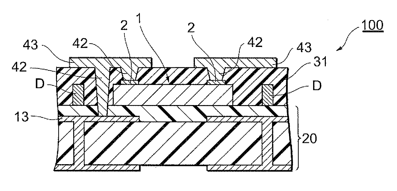
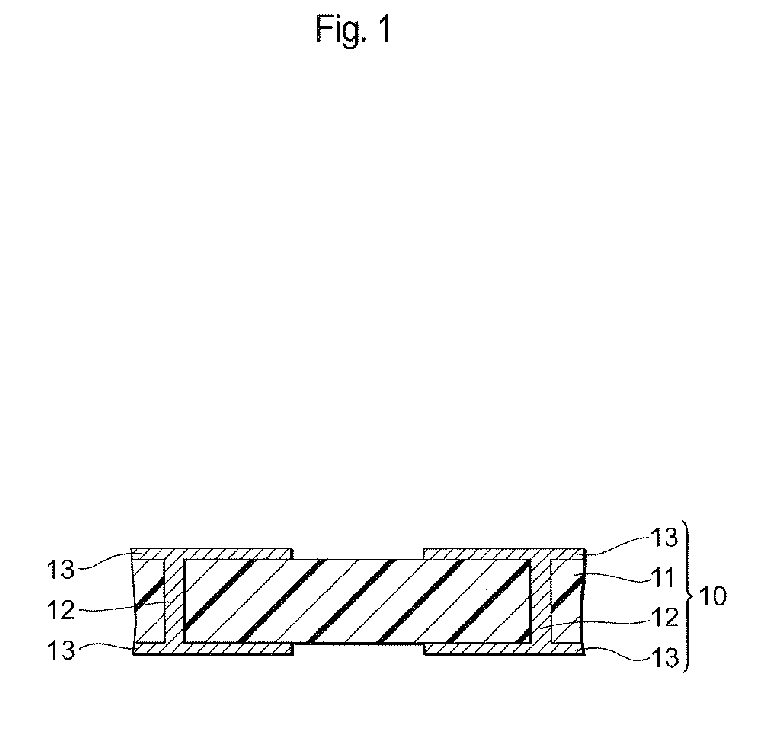
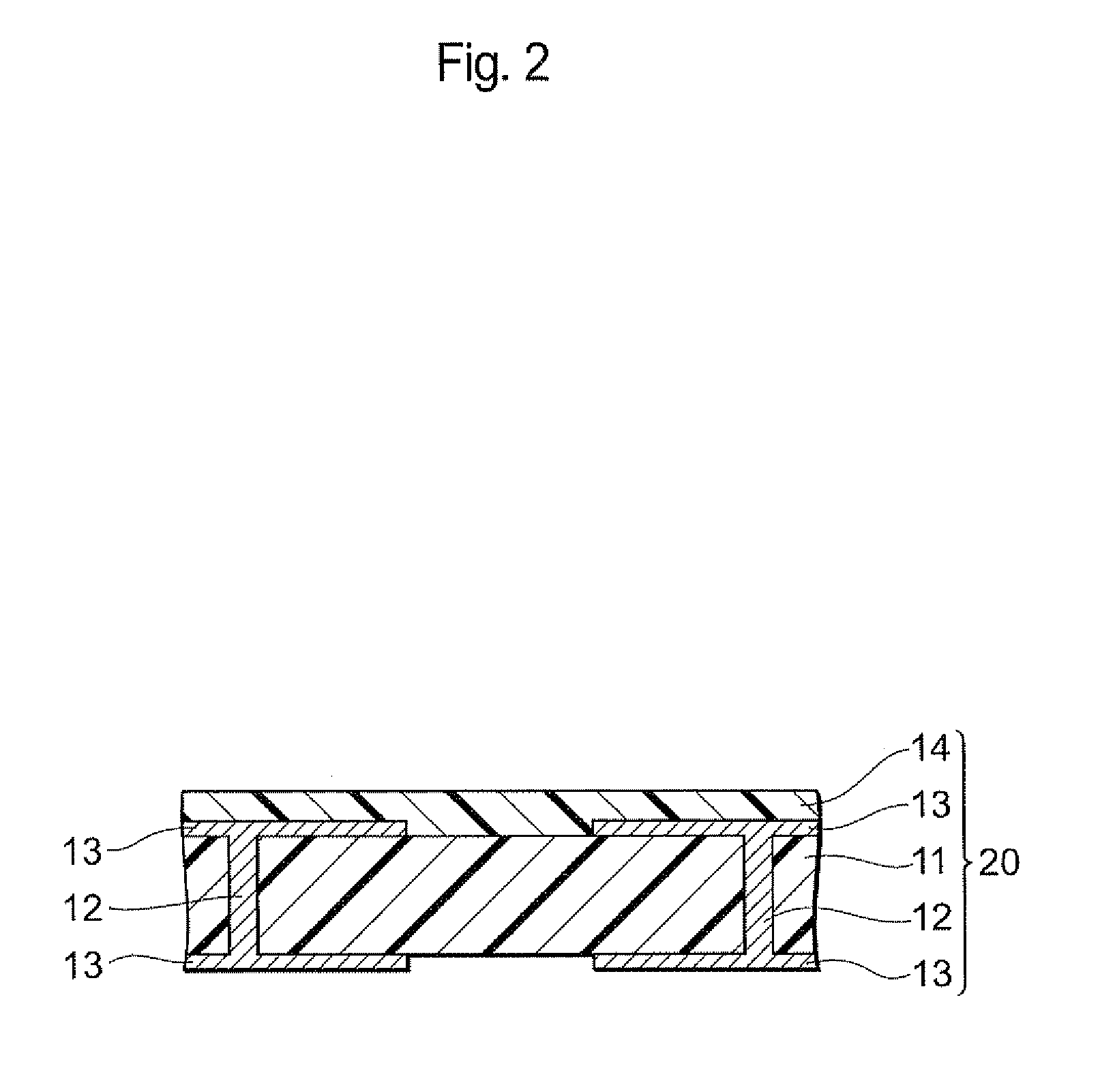
[0028]Hereinafter, embodiments of the present invention will be described in detail. It is to be noted that upper, lower, left and right positional relations and the like are based on positional relations shown in the drawings, unless otherwise specified. Moreover, dimensional ratios of the drawings are not limited to shown ratios. Furthermore, the following embodiments are illustrations for explaining the present invention, and the present invention is not limited only to the embodiments. In addition, the present invention can variously be modified without departing from the scope.

[0029]FIG. 1 to FIG. 10 are process flow diagram (main part enlarged sectional views) showing states where an electronic component-embedded board of the present invention is manufactured according to a suitable embodiment of a method for manufacturing the electronic component-embedded board according to the present invention. Specifically, the process flow diagrams show, as a work board, an example of a m...


PUM

PropertyMeasurementUnit
Electrical resistanceaaaaaaaaaa

Abstract

An electronic component or the like is mounted on a substrate, and on the electronic component, an insulating layer is provided. Afterward, via-holes V are made in the insulating layer on terminals of the electronic component. Each of the terminals of the electronic component has, for example, a laminate structure of a first metal layer, a second metal layer and a third metal layer. When the via-holes V are formed, part of the third metal layer having a comparatively high electric resistance is removed, and the corresponding portion is connected to a wiring layer including via-conductors. Moreover, the third metal layer excellent in close contact properties with the insulating layer is preferably used.

Description

BACKGROUND OF THE INVENTION[0001]1. Field of the Invention[0002]The present invention relates to an electronic component-embedded board, and a method for manufacturing the electronic component-embedded board.[0003]2. Description of the Related Art[0004]In recent years, further miniaturization, thinning, high-density mounting of an electronic apparatus have been demanded. Further miniaturization and thinning have also earnestly been demanded for a circuit board module on which there are mounted electronic components including active components such as a semiconductor device constituted of an IC chip for use in the electronic apparatus, passive components such as a condenser (a capacitor), an inductor (a coil), a thermistor and a resistor, and the like. In recent years, to meet such demands for the miniaturization and thinning, there has been suggested an electronic component-embedded board having a high-density mounting structure where the electronic component is included in the boar...

Claims


Application Information

Patent Timeline
IPC IPC(8): H05K1/09H05K3/32H05K1/16
CPCH01L23/5389Y10T29/49146H01L24/82H01L2924/01012H01L2924/01029H01L23/562H01L2224/04105H01L2224/24227H01L2224/82039H01L2924/3511H01L2224/82031H01L2224/73267H01L23/485H05K1/185H05K3/32H01L2224/32225H01L2224/92244H01L24/24H01L2924/12042H01L2924/00
Inventor TSUYUTANI, KAZUTOSHISUZUKI, YOSHIHIRO
Owner TDK CORPARATION
Learn More