Method for modifying metal cap layers in semiconductor devices

a technology of metal cap layer and semiconductor device, which is applied in the direction of coating, semiconductor device, chemical vapor deposition coating, etc., can solve the problems of affecting the acceptance of this complex process, em and sm have fast become critical challenges, and the defects that can destroy an integrated circuit, so as to improve the effect of em and sm

Inactive Publication Date: 2012-10-04
TOKYO ELECTRON LTD
View PDF5 Cites 50 Cited by
  • Summary
  • Abstract
  • Description
  • Claims
  • Application Information

AI Technical Summary

Benefits of technology

[0006]Embodiments of the invention provide a method for forming a semiconductor device with a modified metal cap layer in Cu metallization to improve electromigration (EM) and stress migration (SM) in the device. The metal cap layer can contain ruthenium (Ru), rhodium (Rh), platinum (Pt), palladium (Pd), or an alloy thereof.

Problems solved by technology

Use of Cu metal in multilayer metallization schemes for manufacturing integrated circuits has created several problems that require solutions.
For example, high mobility of Cu atoms in dielectric materials and Si can result in migration of Cu atoms into those materials, thereby forming electrical defects that can destroy an integrated circuit.
Because electromigration (EM) and stress migration (SM) lifetimes are inversely proportional to current density, EM and SM have fast become critical challenges.
However, maintaining acceptable deposition selectivity on bulk Cu metal, especially for tight pitch Cu wiring, and maintaining good film uniformity, has affected acceptance of this complex process.
Furthermore, wet process steps using acidic solution may be detrimental to the use of CoWP.

Method used


Image

  • Method for modifying metal cap layers in semiconductor devices
  • Method for modifying metal cap layers in semiconductor devices
  • Method for modifying metal cap layers in semiconductor devices

Examples


experimental examples

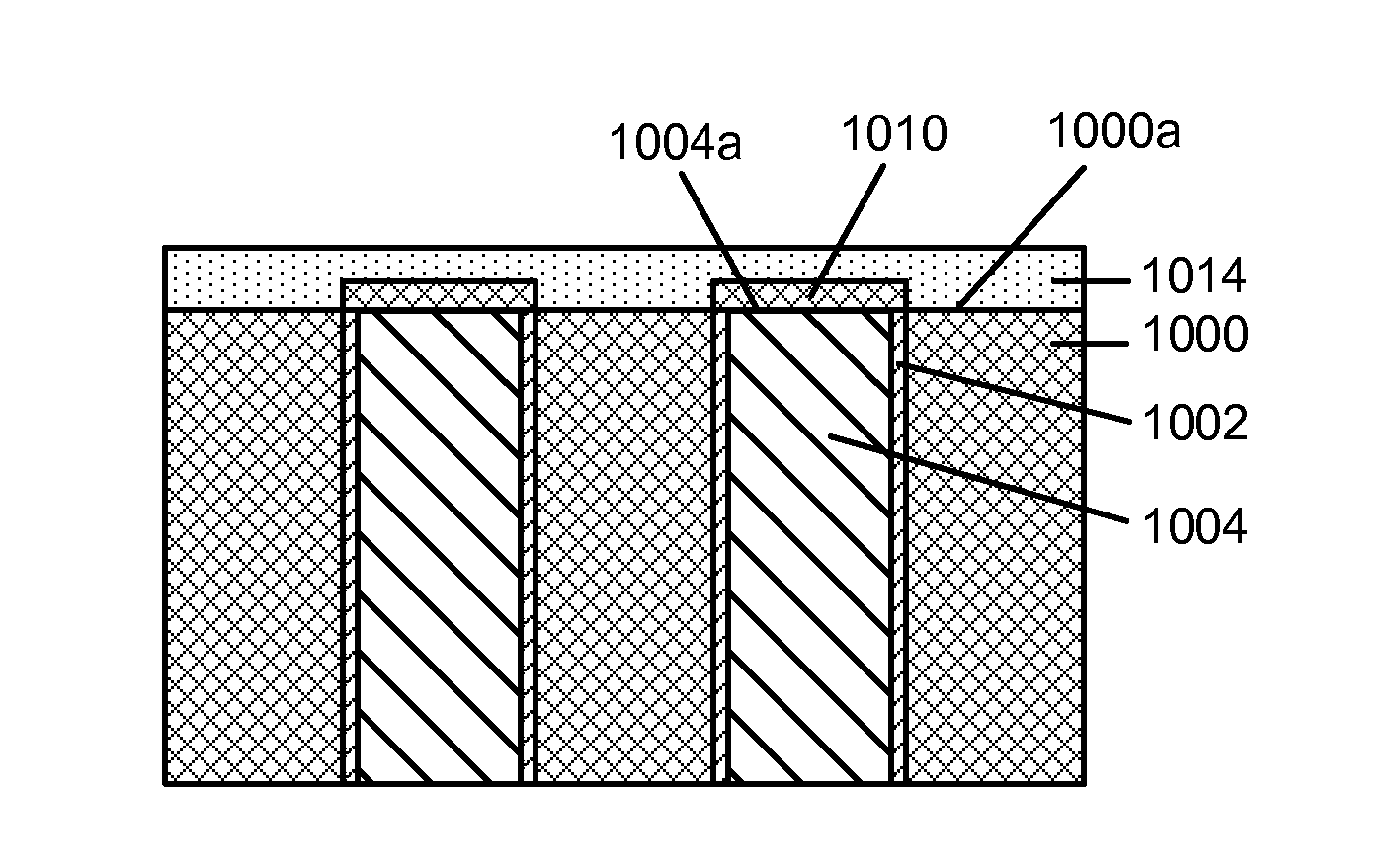
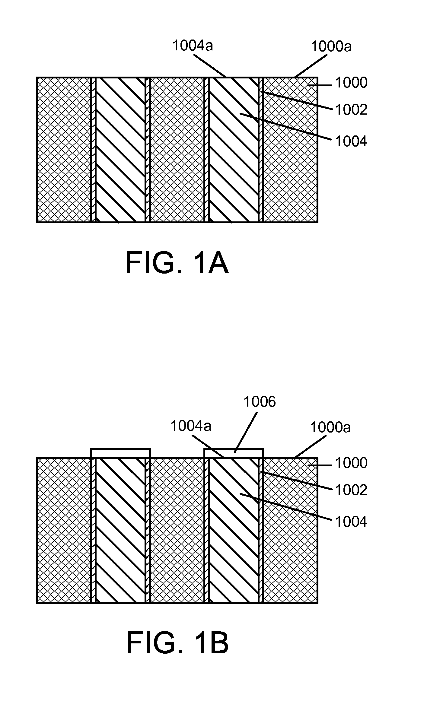
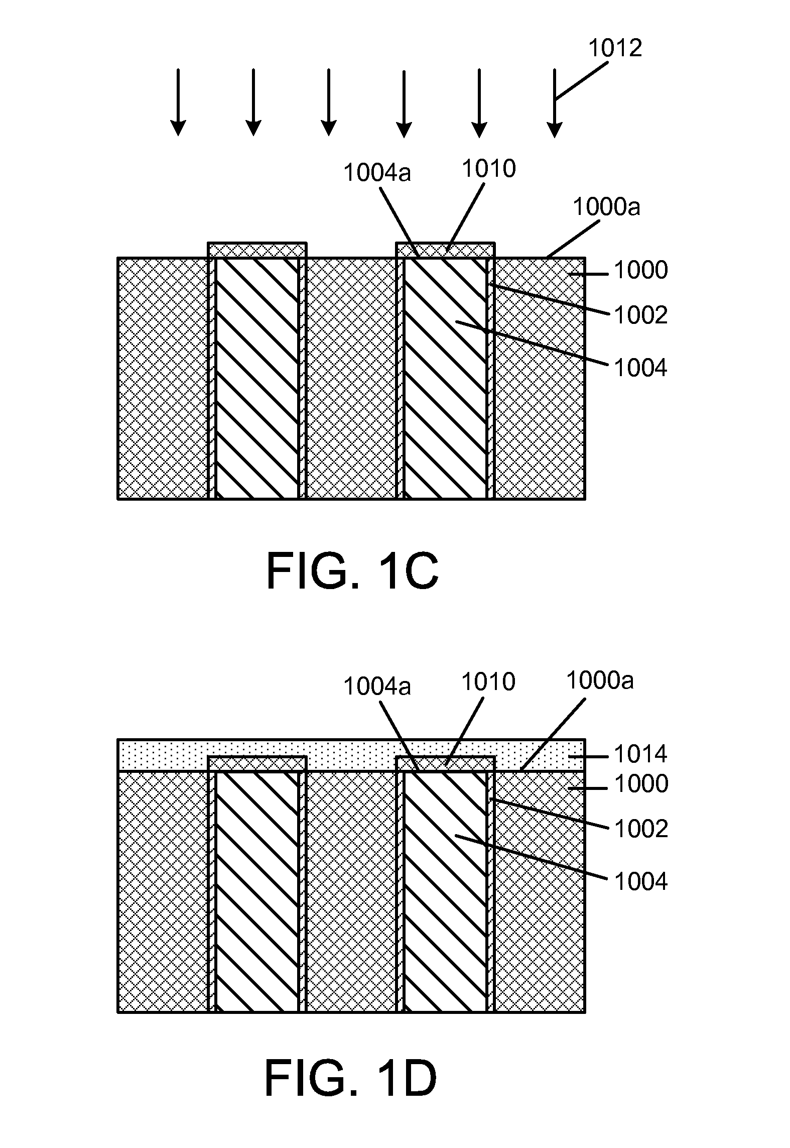
[0034]FIG. 3 shows oxidation resistance results for a dielectric barrier film and a modified Ru metal cap layer according to an embodiment of the invention. The SiCN / Ru / Cu test film structures were formed on 300 mm Si wafers. The experimental matrix included unmodified Ru metal cap layers with thicknesses of 5 nm and 10 nm, Ru metal cap layers with thicknesses of 5 nm and 10 nm modified with NH3 gas exposure without plasma excitation, and SiCN dielectric barrier film thicknesses of 15 nm, 10 nm, 5 nm, and 0 nm (no SiCN dielectric barrier film). The Si wafers with the SiCN / Ru / Cu test structures were subjected to an oxidation barrier test in air at 250° C. for 48 hours. Following the oxidation barrier test, the test structures were evaluated using a scanning electron microscope (SEM) and given a FAILED or PASSED grade. A test structure showing the sign of Cu blistering or film pinholes that indicated oxidation barrier failure of the SiCN / Ru failure received a FAILED grade whereas a te...


PUM

PropertyMeasurementUnit
thicknessaaaaaaaaaa
thicknessaaaaaaaaaa
widthaaaaaaaaaa

Abstract

A method for forming a semiconductor device with improved electromigration (EM) and stress migration (SM) properties. The method includes providing a planarized patterned substrate containing a copper (Cu) metal surface and a low-k dielectric layer surface, selectively depositing a metal cap layer on the Cu metal surface, and modifying the metal cap layer by exposing the metal cap layer to a process gas containing ammonia (NH3) gas without plasma excitation. The method further includes forming a dielectric barrier film on the modified metal cap layer and on the dielectric layer surface, and exposing the dielectric barrier film to a gaseous oxidizing environment, where the dielectric barrier film and the modified metal cap layer prevent oxidation of the Cu metal surface when the dielectric barrier film is exposed to the gaseous oxidizing environment.

Description

FIELD OF THE INVENTION[0001]The present invention relates to semiconductor processing and semiconductor devices, and more particularly, to a method of modifying metal cap layers in copper (Cu) metallization of semiconductor devices to improve electromigration (EM) and stress migration (SM) in bulk Cu metal.BACKGROUND OF THE INVENTION[0002]An integrated circuit contains various semiconductor devices and a plurality of conducting metal paths that provide electrical power to the semiconductor devices and allow these semiconductor devices to share and exchange information. Within the integrated circuit, metal layers are stacked on top of one another using intermetal or interlayer dielectric layers that insulate the metal layers from each other. Normally, each metal layer must form an electrical contact to at least one additional metal layer. Such electrical contact is achieved by etching a hole (i.e., a via) in the interlayer dielectric that separates the metal layers, and filling the r...

Claims


Application Information

Patent Timeline
Patent Type & Authority Applications(United States)
IPC IPC(8): H01L21/28
CPCH01L21/28556H01L21/76834C23C16/52H01L21/76856C23C16/16H01L21/76849
Inventor TOHNOE, KAZUHITO
Owner TOKYO ELECTRON LTD
Why Eureka
Try Eureka