Method for conductively connecting a component on a transparent substrate

Inactive Publication Date: 2012-10-25
SCHOTT AG
View PDF0 Cites 7 Cited by
  • Summary
  • Abstract
  • Description
  • Claims
  • Application Information

AI Technical Summary

Benefits of technology

[0024]An alternative embodiment of the invention may provide that initially connecting points are applied to the conductive layer, for example by means of screen printing or screen process printing or by means of transfer decals. The soldering material is then applied to the connecting points. The soldered connection is then formed between the connecting points and the component. The connecting points may for example consist preferably of a conductive paste or lacquer, for example silver-conductive lacquer or silver-conductive paste. Preferably after application, for example through screen printing, the conductive paste or lacquer is preferably baked on. Baking can at the same time provide pre-tensioning of the transparent substrate, especially the transparent glass substrate. A greater mechanical strength for subsequent process steps is hereby achieved.
[0025]The transparent substrate preferably has a top surface and a bottom surface, whereby the transparent conductive layer is applied onto the top surface and whereby the energy from the energy source, preferably the light source, is radiated from the bottom surface through the transparent substrate, into the material which is to be connected. Radia

Problems solved by technology

Moreover, the possibility of sold

Method used


Image

  • Method for conductively connecting a component on a transparent substrate
  • Method for conductively connecting a component on a transparent substrate

Examples


Example

[0069]Corresponding reference characters indicate corresponding parts throughout the several views. The exemplifications set out herein illustrate embodiments of the invention, and such exemplifications are not to be construed as limiting the scope of the invention in any manner.

DETAILED DESCRIPTION OF THE INVENTION

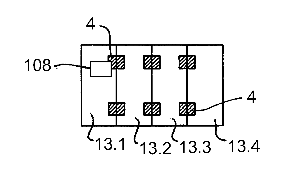
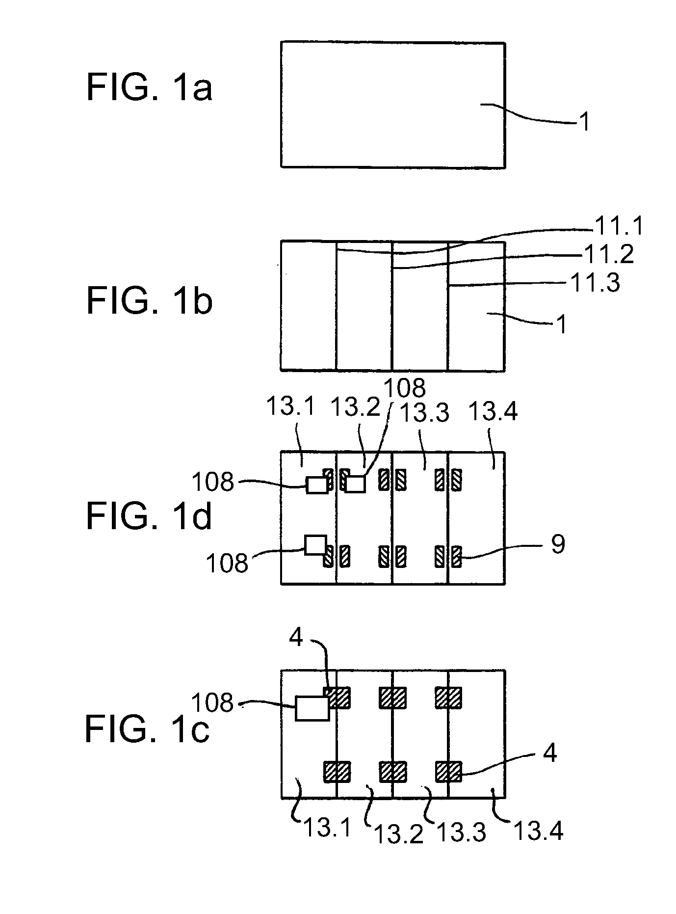
[0070]FIGS. 1a through 1d show a process sequence for the production of a component arrangement, comprising a transparent substrate with transparent conductive layer and components arranged thereupon, in particular light emitting diodes or respectively LED-modules.

[0071]When producing a component arrangement, a substrate 1 with a transparent conductive layer is coated over its entire surface in the illustrated design variation, for example in the sol-gel method (FIG. 1a). The layer is preferably not only a conductive transparent layer, for example an ITO-layer, but a conductive transparent layer which is also heat absorbent. Heat absorbent layers are tin oxide layers, for...


PUM


Abstract

The invention relates to a method to conductively connect an electrical component with at least one conductive layer, whereby the conductive layer is applied to a substrate which is essentially transparent in the visible wavelength zone of light, comprising the following steps: the electrical component or the conductive layer is provided with a soldering material in the area where the component is to be connected to the conductive layer; the soldering material is provided with energy supplied by an energy source, such that the soldering material melts and a non-detachable, material-bonded conductive connection between the electrical component and the conductive layer is established.

Description

CROSS-REFERENCE TO RELATED APPLICATIONS[0001]This is a continuation of PCT application No. PCT / EP2010 / 001961, entitled “METHOD FOR CONDUCTIVELY CONNECTING A COMPONENT ON A TRANSPARENT SUBSTRATE”, filed Mar. 27, 2010, which is incorporated herein by reference.BACKGROUND OF THE INVENTION[0002]1. Field of the Invention[0003]The invention relates to a method for conductively connecting an electrical component having at least one conductive layer, whereby the conductive layer is applied to a substrate which is essentially transparent in the visible wavelength zone of light. In the current application “visible wavelength” is to be understood to represent that the transmission between 420 nm and 700 nm of the layer or respectively the substrate is greater than 60%, especially greater than 80%, preferably greater than 90%.[0004]2. Description of the Related Art[0005]It is known from the current state of the art, in particular from WO 01 / 82378 to install components, in particular light emitt...

Claims


Application Information

Patent Timeline
IPC IPC(8): H05K3/34
CPCB23K1/0016Y10T29/49149B23K26/365B23K26/367B23K26/4005B23K26/401B23K26/402B23K26/409B23K35/268B23K35/3602B23K2201/42H05K1/0306H05K3/341H05K3/3494H05K2201/0108H05K2201/0112H05K2201/0326H05K2201/10106H05K2203/107B23K1/005Y10T29/49142Y10T29/49144H01L2924/12041H01L24/81H01L2224/81192H01L2224/81224H01L2224/97H01L2224/81H01L2924/00B23K26/40B23K26/361B23K26/364B23K2101/42B23K2103/172B23K2103/18B23K2103/50B23K2103/52B23K2103/54H01L2924/12042H01L2924/15788H05K3/34
Inventor NICKUT, ANDREASALBRECHT, BERNDKRACHT, PETER
Owner SCHOTT AG
Why Eureka
Try Eureka