Nonvolatile variable resistive element and nonvolatile semiconductor memory device

Inactive Publication Date: 2012-10-25
SHARP KK +1
View PDF1 Cites 52 Cited by
  • Summary
  • Abstract
  • Description
  • Claims
  • Application Information

AI Technical Summary

Benefits of technology

[0043]Therefore, according to the present invention, the nonvolatile variable resistive element can perform the reading operation by the low reading voltage, reduce a cell area, and be easily pr

Problems solved by technology

However, recently it has been found that the flash memory is limited in its miniaturization, so that nonvolatile memories such as a MRAM (Magnetoresistive Random Access Memory), a PCRAM (Phase Change Random Access Memory), a CBRAM (Conductive Bridging Random Access Memory), and a RRAM (Resistive Random Access Memory: Refer to A. Sawa, “Resistive switching in transition metal oxides”, Material Today, Vol. 11, No. 6, p.
However, the leak current can be prevented to a certain degree by this method, but in order to effectively prevent the leak current, it is necessary to reduce the number of the elements to the relatively small number in the memory cell array, so that area occupied by the decoder increases, and a memory chip size cannot be reduced.
The 1T1R structure can control an amount and a direction of a current flowing in the variable resistive element

Method used


Image

  • Nonvolatile variable resistive element and nonvolatile semiconductor memory device
  • Nonvolatile variable resistive element and nonvolatile semiconductor memory device
  • Nonvolatile variable resistive element and nonvolatile semiconductor memory device

Examples


first embodiment

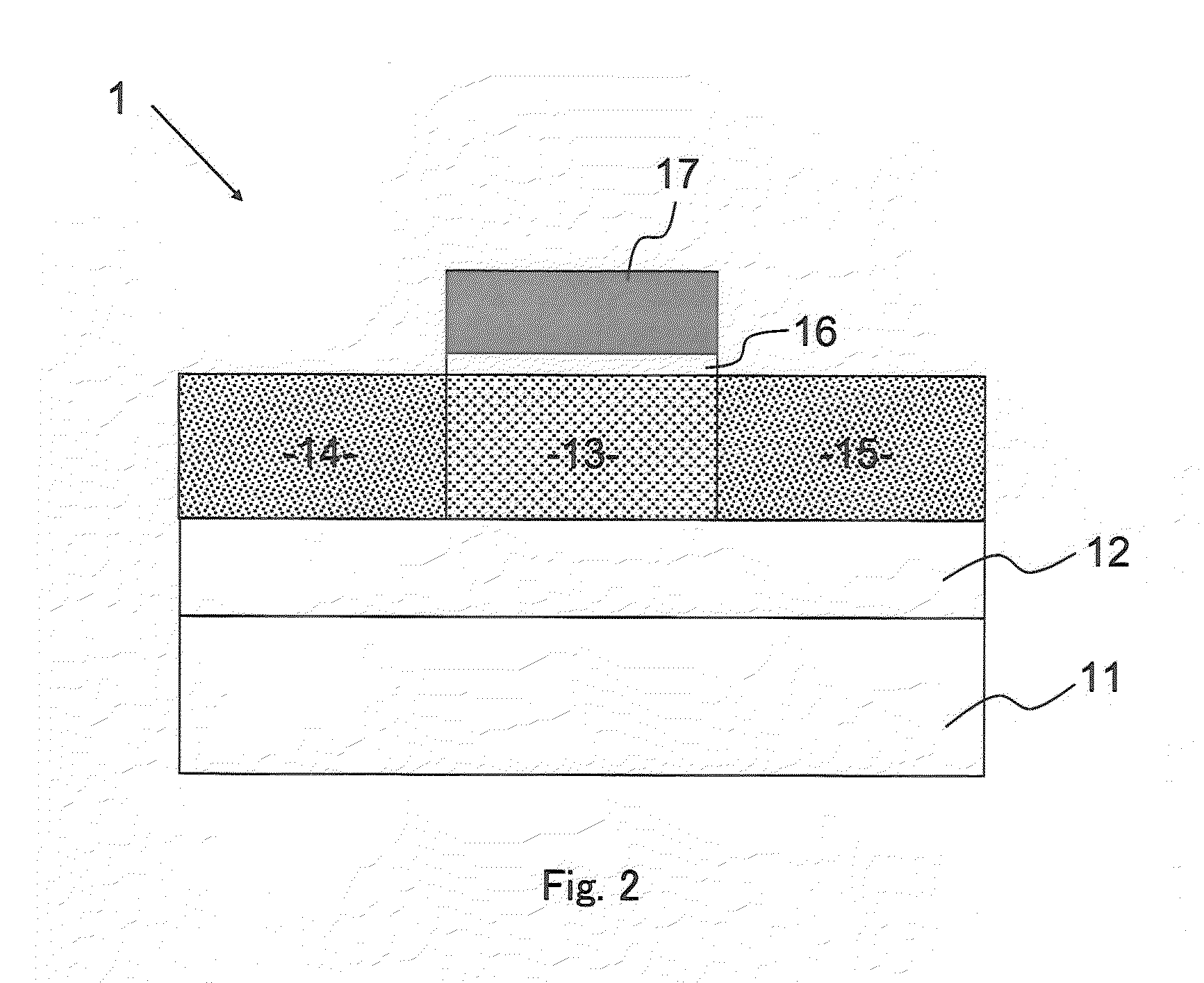
[0076]FIG. 2 is a cross-sectional view of an element structure of a nonvolatile variable resistive element according to a first embodiment of the present invention (hereinafter, referred to as the element 1 of the present invention). In addition, a substantial part is overdrawn in the following drawings for convenience of description, so that a dimensional ratio of each part of the element does not always coincide with an actual dimensional ratio.

[0077]As shown in FIG. 2, the element 1 of the present invention has metal oxide films 13, 14, and 15 formed on an interlayer insulation film 12 on a substrate 11, an insulation film 16 formed in a predetermined region on the metal oxide films 13 to 15, and a gate electrode (third electrode) 17 formed on the insulation film 16. The metal oxide film 13 is composed of a metal oxide which causes a resistance change depending on an oxide concentration in the film. When a voltage not lower than a threshold value is applied from the gate electrod...

second embodiment

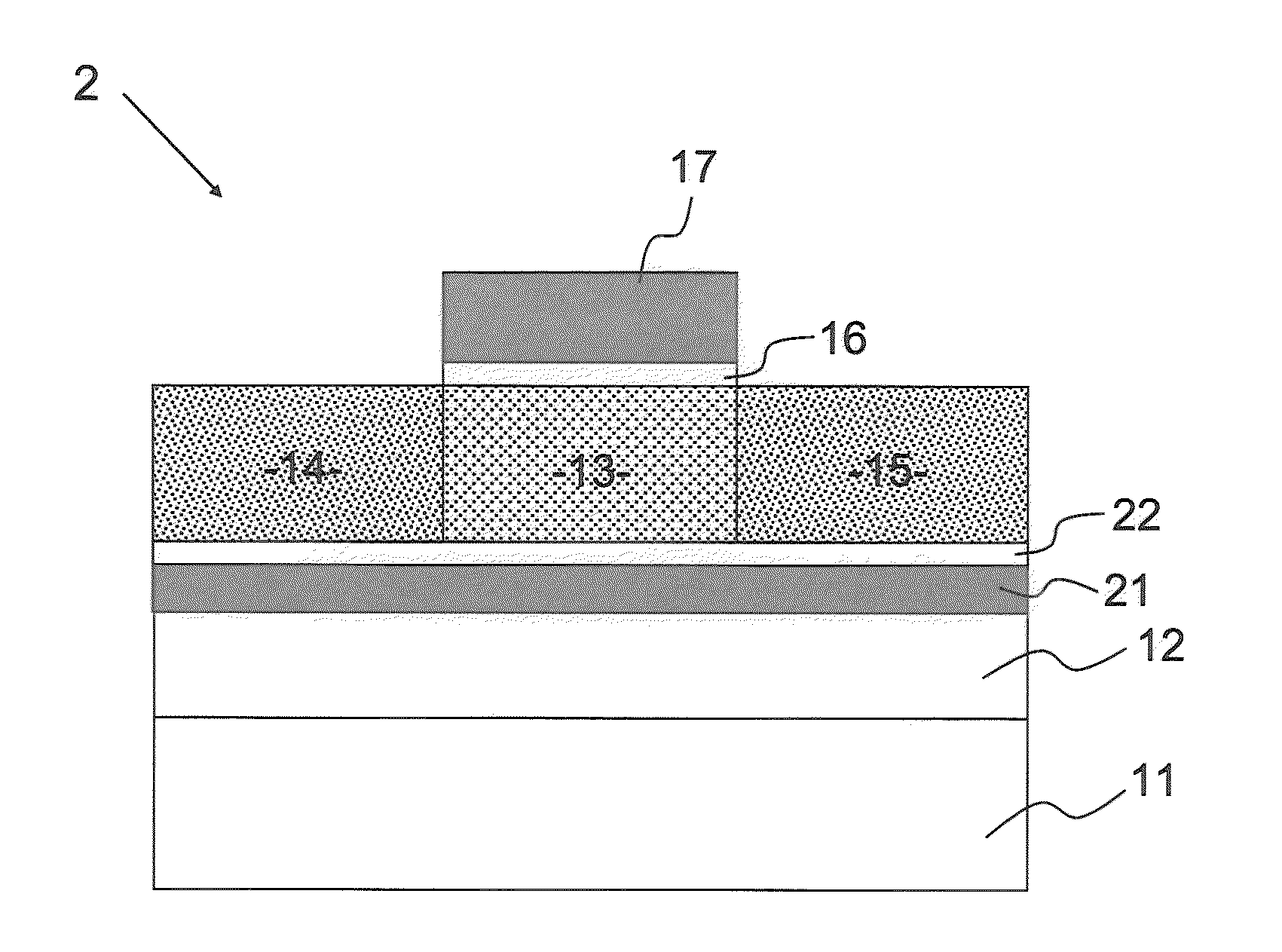
[0096]FIG. 6 is a cross-sectional view of an element structure of a nonvolatile variable resistive element according to a second embodiment of the present invention (hereinafter, referred to as the element 2 of the present invention). The element 2 of the present invention further includes an electrode to supply a writing voltage from the side of a substrate, in addition to the components of the element 1 of the present invention, that is, the nonvolatile variable resistive element has a four-terminal structure.

[0097]As shown in FIG. 6, the element 2 of the present invention is provided such that a second gate electrode (fourth electrode) 21 is formed on the interlayer insulation film 12 on the substrate 11, and the metal oxide films 13, 14, and 15 are formed on the second gate electrode 21 with a second insulation film 22 interposed therebetween. The insulation film 16 is formed in a predetermined region on the metal oxide films 13 to 15, and the gate electrode (third electrode) 17...

third embodiment

[0111]FIG. 10 is a cross-sectional view of an element structure of a nonvolatile variable resistive element according to a third embodiment of the present invention (hereinafter, referred to as the element 3 of the present invention).

[0112]The element 3 of the present invention has a structure in which the annular metal oxide films 13, 14, and 15 are laminated in an axial direction, and the annular insulation film 16 is formed on outer side wall surfaces of the annular metal oxide films 13 to 15, and the annular second insulation film 22 is formed on inner side wall surfaces of the annular metal oxide films 13 to 15. That is, the element 3 of the present invention is formed in a cylindrical shape having a three-layer structure in which the second insulation film 22, the metal oxide films 13 to 15, and the insulation film 16 are formed from the inner side in this order, and the plate-shaped gate electrode (third electrode) 17 is formed into a layer shape perpendicular to an axial dir...


PUM


Abstract

A large-capacity and inexpensive nonvolatile semiconductor memory device that prevents a leak current and is operated at high speed is implemented with a nonvolatile variable resistive element. A memory cell array includes the nonvolatile variable resistive elements each including a variable resistor composed of a metal oxide film to cause a resistance change according to an oxygen concentration in the film, an insulation film formed on the variable resistor, first and second electrodes to sandwich the variable resistor, and a third electrode opposite to the variable resistor across the insulation film. A writing operation is performed by applying a voltage to the third electrode to induce an electric field having a threshold value or more, in a direction perpendicular to an interface between the variable resistor and the insulation film, and a resistance state of the variable resistor is read by applying a voltage between the first and second electrodes.

Description

CROSS REFERENCE TO RELATED APPLICATION[0001]This Nonprovisional application claims priority under 35 U.S.C. §119(a) on Patent Application No. 2010-099688 filed in Japan on Apr. 23, 2010 the entire contents of which are hereby incorporated by reference.1. FIELD OF THE INVENTION[0002]The present invention relates to a semiconductor memory device and more particularly to a nonvolatile semiconductor memory device including a nonvolatile variable resistive element having a first terminal, a second terminal, and a variable resistor formed on a current path between the terminals, and capable of reversibly changing a resistance state defined by electric resistance between the terminals, between two or more different states in response to an applied voltage and holding it.2. DESCRIPTION OF THE RELATED ART[0003]In tandem with the penetration of a mobile device such as a portable electric device, a flash memory has been widely used as a large-capacity and inexpensive nonvolatile memory which c...

Claims


Application Information

Patent Timeline
IPC IPC(8): G11C11/00H01L45/00
CPCG11C13/0007G11C2213/53G11C2213/75H01L27/101H01L45/08H01L27/2481H01L45/1226H01L45/1233H01L45/147H01L27/2472H01L45/1206H10B63/82H10B63/84H10N70/253H10N70/24H10N70/823H10N70/8836H10N70/826
Inventor AWAYA, NOBUYOSHITAMAI, YUKIOSAWA, AKIHITO
Owner SHARP KK
Why Eureka
Try Eureka