Semiconductor memory device

Inactive Publication Date: 2012-11-01
SEMICON ENERGY LAB CO LTD
View PDF9 Cites 8 Cited by
  • Summary
  • Abstract
  • Description
  • Claims
  • Application Information

AI Technical Summary

Benefits of technology

[0021]According to one embodiment of the present invention, a CAM including a nonvolatile memory device that consumes low power can be achieved. According to one embodiment of th

Problems solved by technology

This poses a problem of increased power consumption.
Moreover, the CAM including a nonvolatile memory device to which data is written by feeding current has a problem of degradation due to repeated writing.
Furthermore, t

Method used


Image

  • Semiconductor memory device
  • Semiconductor memory device
  • Semiconductor memory device

Examples


embodiment 1

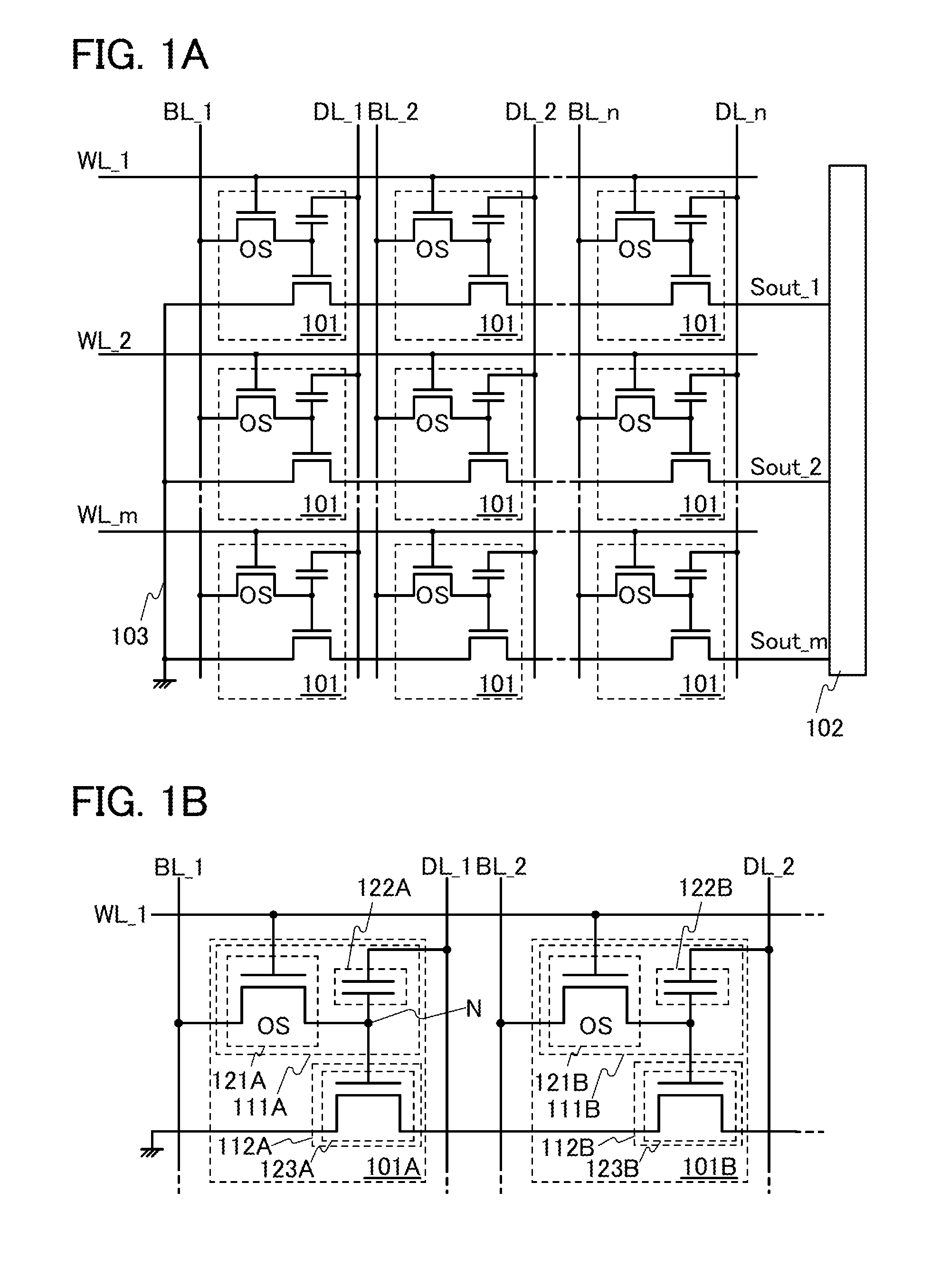
[0041]This embodiment describes the structure of a semiconductor memory device that can act as a CAM with reference to FIGS. 1A and 1B.

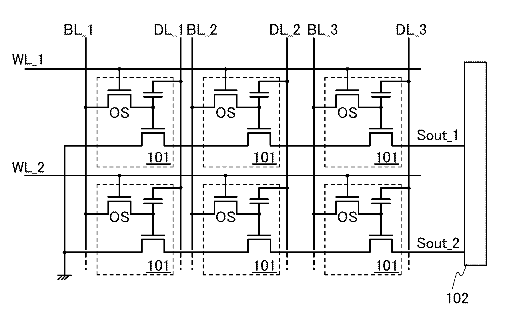
[0042]FIG. 1A is a circuit diagram of a semiconductor memory device including m rows and n columns (m and n are natural numbers) of memory cells. The semiconductor memory device in FIG. 1A includes bit lines BL_1 to BL_n, word lines WL_1 to WL_m, data lines DL_1 to DL_n, a plurality of memory cells 101, and a determination circuit 102.

[0043]The memory cell 101 is connected to any one of the bit lines BL_1 to BL_n, any one of the word lines WL_1 to WL_m, and any one of the data lines DL_1 to DL_n. In addition, memory cells 101 are connected in the row direction, that is, the direction in which the word lines WL_1 to WL_m are extended. One terminal of each of output signal lines Sout_1 to Sout_m is connected to the determination circuit 102, and the other terminal is connected to a common power supply line 103 (a GND line in FIG. 1A).

[0044]The determin...

embodiment 2

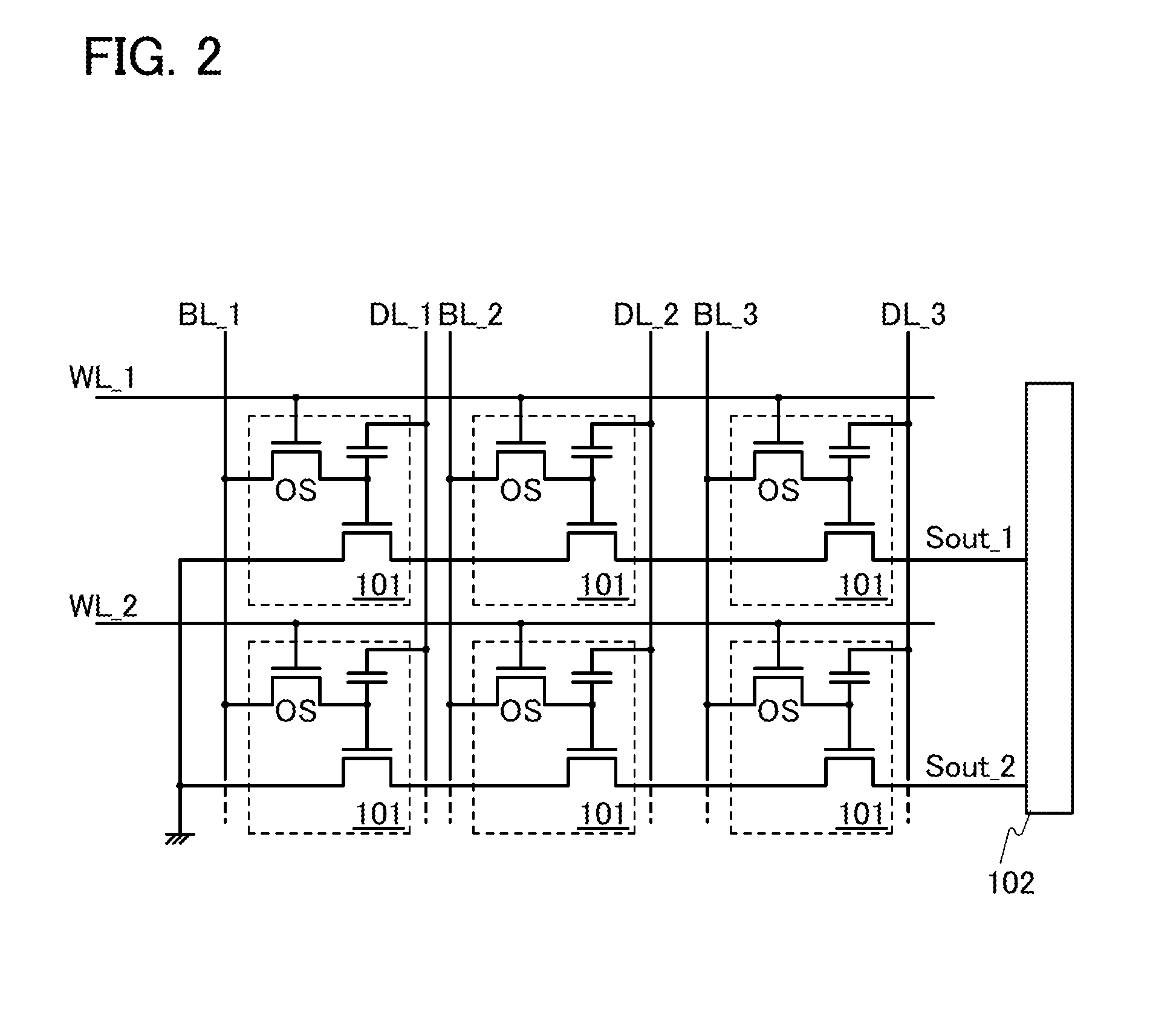
[0066]This embodiment shows a specific structure of the semiconductor memory device in Embodiment 1 which can act as a CAM, and examples of the structure and operation of the semiconductor memory device with reference to FIG. 2, FIGS. 3A and 3B, FIGS. 4A and 4B, and FIGS. 5A and 5B.

[0067]FIG. 2 is a circuit diagram of a semiconductor memory device including two rows and three columns of memory cells, which is shown as an example of the semiconductor memory device in FIG. 1A. The semiconductor memory device in FIG. 2 includes bit lines BL_1 to BL_3, word lines WL_1 and WL_2, data lines DL_1 to DL_3, two rows and three columns of memory cells 101, and the determination circuit 102. Connections between each memory cell 101 and the lines, and the circuit configuration of the memory cells are similar to those in FIGS. 1A and 1B.

[0068]Next, a description is given with reference to FIGS. 3A and 3B of an operation for writing data to each row in the semiconductor memory device illustrated i...

embodiment 3

[0085]This embodiment shows a plurality of modes of the structure of the second transistor in the reference circuit described in Embodiment 1.

[0086]As described in the above embodiment, detection of the conducting state or nonconducting state of the second transistor enables high-speed data search. Therefore, unlike a semiconductor layer in the first transistor, a semiconductor layer in the second transistor can be formed using various materials.

[0087]For example, like FIG. 1A, FIG. 6A is a circuit diagram illustrating a configuration of a memory cell. FIG. 6A illustrates a first transistor 131, a capacitor 132, and a second transistor 133A. A semiconductor layer in the second transistor 133A can be formed using silicon.

[0088]Note that silicon for the semiconductor layer can be microcrystalline silicon, polycrystalline silicon, single crystal silicon, or the like. Note that in FIG. 6A, the second transistor 133A is represented by “Si” so that it is regarded as a transistor whose cha...


PUM


Abstract

An object is to provide a semiconductor memory device that enables low power consumption of a memory cell of a CAM including a nonvolatile memory device. Another object is to provide a semiconductor memory device without degradation due to repeated data writing. Still another object is to provide a nonvolatile memory device that enables high density of memory cells. A semiconductor memory device is provided which includes a memory circuit including a first transistor including an oxide semiconductor in a semiconductor layer, and a capacitor in which a potential corresponding to written data can be retained by turning off the first transistor; and a reference circuit for referring the written potential. The semiconductor memory device enables a high-speed search function by obtaining the address of data generated by detecting the conducting state of a second transistor in the reference circuit.

Description

BACKGROUND OF THE INVENTION[0001]1. Field of the Invention[0002]The present invention relates to a semiconductor memory device, particularly to a semiconductor memory device that enables high-speed search of data to be searched stored in the semiconductor memory device.[0003]2. Description of the Related Art[0004]A content addressable memory (hereinafter called CAM) is a semiconductor memory device that enables high-speed search by obtaining the address of data generated by comparing stored data with data to be searched, unlike a semiconductor memory device in which stored data is read by addressing.[0005]Examples of CAMs include a structure using a volatile memory device as described in Patent Document 1. In a CAM using a volatile memory device, stored data is lost when the supply of a supply voltage is stopped. Particularly in mobile devices which cannot be easily supplied with the supply voltage stably, the loss of data caused by stopping the supply of the supply voltage causes i...

Claims


Application Information

Patent Timeline
IPC IPC(8): H01L29/94
CPCH01L27/1156H01L27/1207G11C15/046H01L29/263G11C7/16H01L27/108G11C7/12H10B41/70H10B12/00
Inventor TAKAHASHI, YASUYUKI
Owner SEMICON ENERGY LAB CO LTD
Why Eureka
Try Eureka