Defect detection method and defect detection device and defect observation device provided with same

Active Publication Date: 2012-11-01
HITACHI HIGH-TECH CORP
View PDF9 Cites 53 Cited by
  • Summary
  • Abstract
  • Description
  • Claims
  • Application Information

AI Technical Summary

Benefits of technology

[0020]According to the present invention, when precisely observing, by an SEM or the like, the defect detected by an optical defect inspection device, it is possible to surely place the defect as the observation target in the observation visual field of the SEM; hence, it is po

Problems solved by technology

For example, in a production process of semiconductor devices, presence of foreign matter or pattern defects such as a short-circuit and a disconnection (defects described hereinafter include foreign matter and pattern defects) on a semiconductor substrate (wafe

Method used


Image

  • Defect detection method and defect detection device and defect observation device provided with same
  • Defect detection method and defect detection device and defect observation device provided with same
  • Defect detection method and defect detection device and defect observation device provided with same

Examples


second embodiment

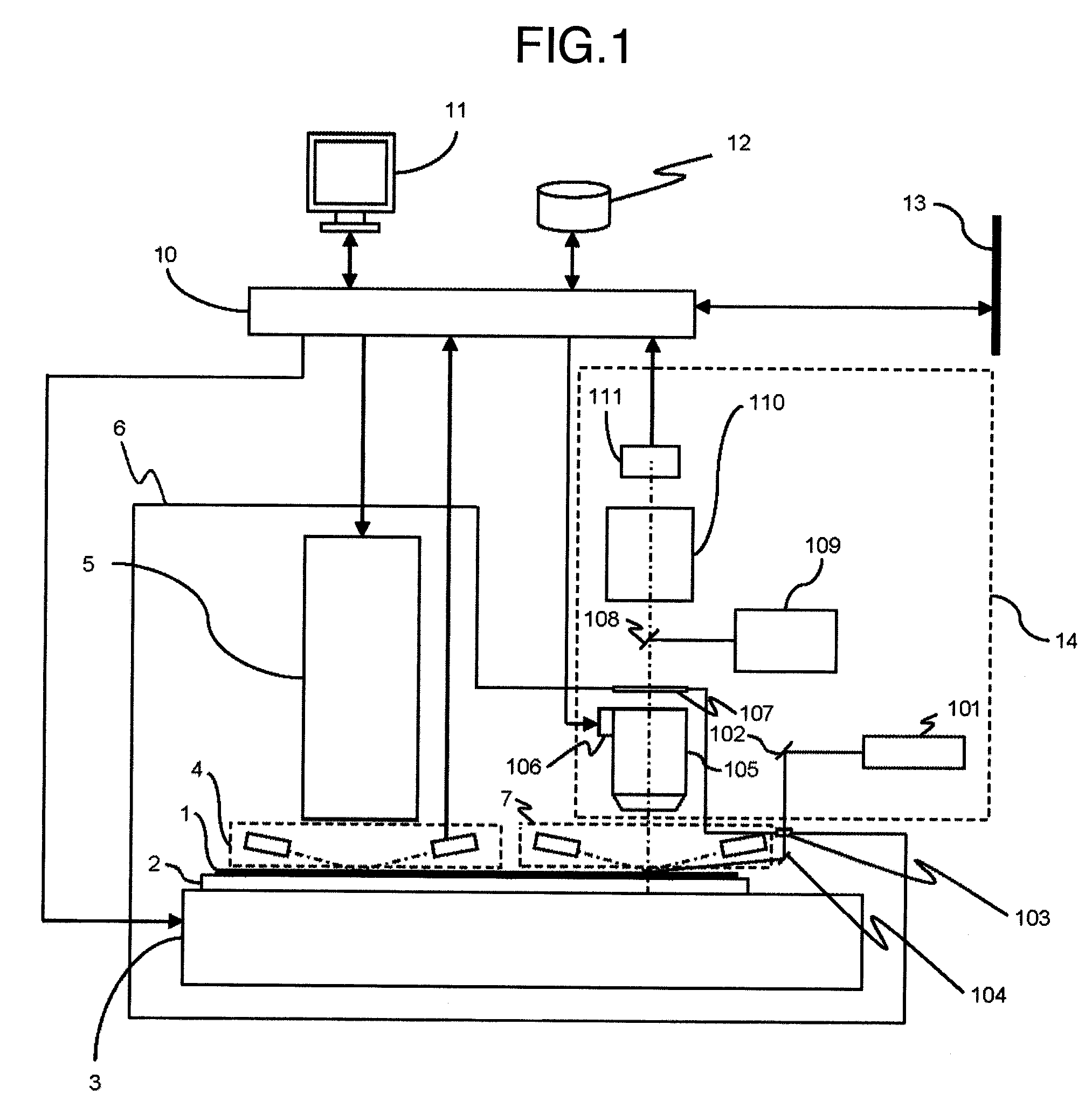
[0125]Next, description will be given of a second embodiment of the defect inspection device according to the present invention by referring to FIG. 18. The second embodiment differs from the first embodiment in that the half-silvered mirror 108 and the bright-field lighting unit 109 are not arranged. Hence, the configuration is advantageously simplified as shown in FIG. 18. In the configuration shown in FIG. 18, the components assigned with the same reference numerals as those of the configuration of FIG. 1 have functions similar to those described by referring to FIG. 1.

[0126]In this situation, the focusing of the optical microscope 14 is carried out by use of the Z sensor 7 or through image processing based on dark-field images obtained by the optical microscope 14 as described above.

[0127]In this case, as in the optical microscope 14 shown in FIG. 16, the distribution polarization element 114 may be fixed onto the pupil plane 112a of the objective 105 in the configuration.

third embodiment

[0128]Next, description will be given of a third embodiment of the defect inspection device according to the present invention by referring to FIG. 19. The third embodiment differs from the first embodiment in that the Z sensor 7, the half-silvered mirror 108, and the bright-field lighting unit 109 are not arranged for the optical microscope 14. Hence, advantageously, the configuration is simplified as shown in FIG. 19 and there is secured a space in which an objective having a larger numeral aperture is installed as the objective 105. In the configuration shown in FIG. 19, the components assigned with the same reference numerals as those of the configuration of FIG. 1 have functions similar to those described by referring to FIG. 1.

[0129]In this configuration, the focusing of the optical microscope 14 is carried out by use of the Z sensor 7 or through image processing based on dark-field images obtained by the optical microscope 14 as described above.

[0130]In this occasion, as in t...

fourth embodiment

[0131]Next, description will be given of a fourth embodiment of the defect inspection device according to the present invention by referring to FIG. 20. The fourth embodiment differs from the first embodiment in that the Z sensor 7 is not arranged for the optical microscope 14. Hence, advantageously, the configuration is simplified as shown in FIG. 20, and there is secured a space in which an objective having a larger numeral aperture is installed as the objective 105. In the configuration shown in FIG. 20, the components assigned with the same reference numerals as those of the configuration of FIG. 1 have functions similar to those described by referring to FIG. 1.

[0132]In this case, the focusing of the optical microscope 14 is carried out through image processing based on bright-field images or dark-field images obtained by the optical microscope 14 as described above.

[0133]In the configuration, as in the optical microscope 14 shown in FIG. 16, the distribution polarization eleme...


PUM


Abstract

The disclosed device, which, using an electron microscope or the like, minutely observes defects detected by an optical appearance-inspecting device or an optical defect-inspecting device, can reliably insert a defect to be observed into the field of an electron microscope or the like, and can be a device of a smaller scale. The electron microscope (5), which observes defects detected by an optical appearance-inspecting device or by an optical defect-inspecting device, has a configuration wherein an optimal microscope (14) that re-detects defects is incorporated, and a spatial filter and a distribution polarization element are inserted at the pupil plane when making dark-field observations using this optical microscope (14). The electron microscope (5), which observes defects detected by an optical appearance-inspecting device or an optical defect-inspecting device, has a configuration wherein an optimal microscope (14) that re-detects defects is incorporated, and a distribution filter is inserted at the pupil plane when making dark-field observations using this optical microscope (14).

Description

TECHNICAL FIELD[0001]The present invention relates to a defect detection method, a defect detection device, and a defect observation device including the same for inspecting defects and the like on a surface of a bare wafer without semiconductor patterns or a filmed wafer without semiconductor patterns or on a surface of a disk.BACKGROUND ART[0002]For example, in a production process of semiconductor devices, presence of foreign matter or pattern defects such as a short-circuit and a disconnection (defects described hereinafter include foreign matter and pattern defects) on a semiconductor substrate (wafer) causes failures including an insulation failure and a short-circuit in the wiring. Further, as the circuit pattern formed on a wafer becomes finer, a finer defect also causes an insulation failure in a capacitor and destruction of a gate oxide film or the like. As for defects, matter appearing from a movable unit of a transporting device, matter generating from a human body, matt...

Claims


Application Information

Patent Timeline
IPC IPC(8): G01N21/88
CPCG01N21/21G01N21/9501G01N2021/8822G01N21/95623G01N21/95607G01N21/47G01N2201/06113G01N2201/063G01N21/8806G01N21/94G01N2021/8848
Inventor OTANI, YUKOTACHIZAKI, TAKEHIROWATANABE, MASAHIROMATSUMOTO, SHUNICHI
Owner HITACHI HIGH-TECH CORP
Why Eureka
Try Eureka