Semiconductor device
a technology of semiconductor devices and display devices, applied in pulse generators, pulse techniques, instruments, etc., can solve problems such as failure of driver circuits, failure of transistors, and degradation of operating frequency ranges, so as to reduce the vgs of transistors, prevent circuit malfunctions, and reduce drain current of transistors in the off-state
- Summary
- Abstract
- Description
- Claims
- Application Information
AI Technical Summary
Benefits of technology
Problems solved by technology
Method used
Image

Examples
embodiment 1
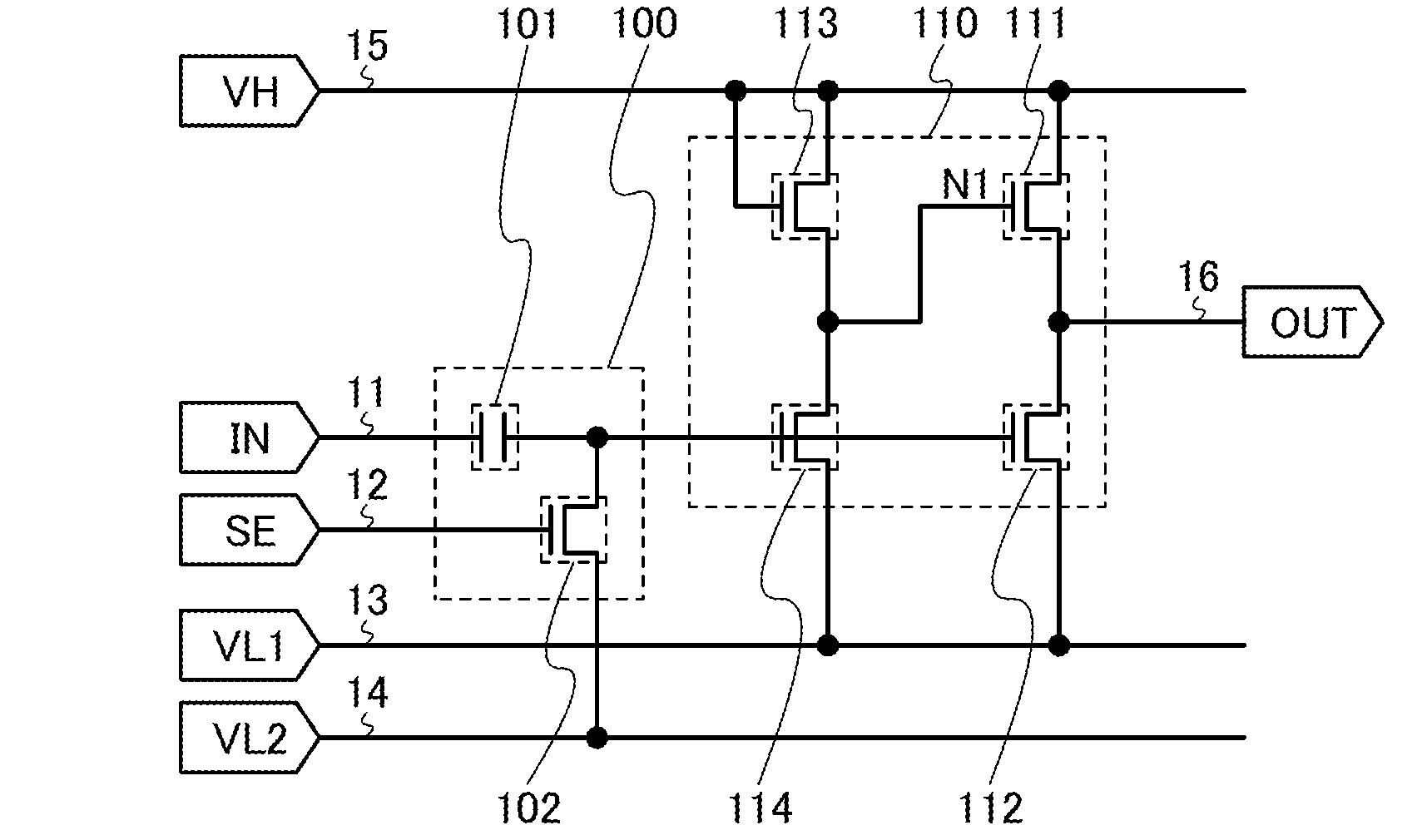
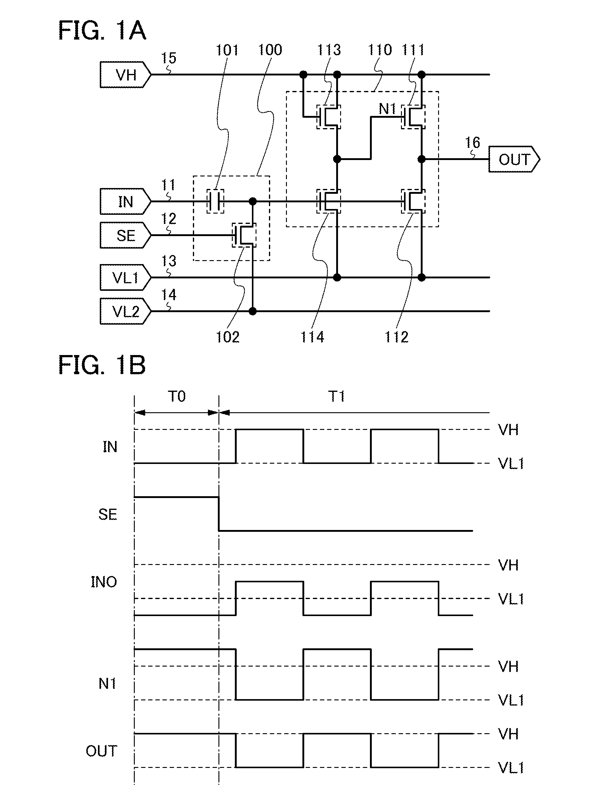
[0039]In this embodiment, one example of a semiconductor device which is driven by a signal generated by offsetting an input signal is described.
[0040]A configuration of a semiconductor device of this embodiment is described with reference to FIG. 1A. FIG. 1A is a circuit diagram of the semiconductor device of this embodiment. The semiconductor device in FIG. 1A includes a circuit 100 and a circuit 110. The circuit 100 is connected to a wiring 11, a wiring 12, a wiring 14, and the circuit 110. The circuit 110 is connected to a wiring 15, a wiring 13, a wiring 16, and the circuit 100. The wirings and the like connected to any of the circuits 100 and 110 can be changed as appropriate depending on the configurations of the circuits 100 and 110.
[0041]Note that in this specification, the case where X and Y are electrically connected to each other, the case where X and Y are functionally connected to each other, and the case where X and Y are directly connected to each other are encompass...
embodiment 2
[0110]In this embodiment, the case where the semiconductor device which is one embodiment of the present invention is used for a flip-flop circuit included in a shift register is described. Description is made on portions different from Embodiment 1.
[0111]The semiconductor device of this embodiment is described with reference to FIG. 6A. FIG. 6A is a circuit diagram of the semiconductor device of this embodiment. The semiconductor device in FIG. 6A is different from that shown in FIG. 1A in that the first terminal of the transistor 111 is connected to a wiring 23, the gate of the transistor 113 is connected to a wiring 21, and the one electrode of the capacitor 101 is connected to a wiring 22.
[0112]Signal IN1 is input to the wiring 21. The signal IN1 is an input signal of the semiconductor device and serves as a start pulse. For example, the signal IN1 is a digital signal whose high-level potential is VH and low-level potential is VL1. The wiring 21 transmits the signal IN1.
[0113]Si...
embodiment 3
[0158]In this embodiment, a shift register in which the semiconductor device described in Embodiment 2 is used as a flip-flop circuit is described. Description is made on portions different from Embodiments 1 and 2.
[0159]The shift register of this embodiment is described with reference to FIG. 11. FIG. 11 is a circuit diagram of the shift register of this embodiment. The shift register in FIG. 11 includes N flip-flop circuits 200 (N is a natural number). Among these, 1st to 3rd stage flip-flop circuits 200 (denoted by a flip-flop circuit 200_1, a flip-flop circuit 200_2, and a flip-flop circuit 200_3) are shown in FIG. 11.
[0160]In the shift register shown in FIG. 11, the semiconductor device shown in FIG. 6A is used as the flip-flop circuit 200. However, the flip-flop circuit 200 is not limited to the semiconductor device shown in FIG. 6A and any other semiconductor device described in Embodiment 2 can be used as appropriate.
[0161]Connection relations in the shift register circuit s...
PUM
| Property | Measurement | Unit |
|---|---|---|
| specific resistivity | aaaaa | aaaaa |
| specific resistivity | aaaaa | aaaaa |
| Ra | aaaaa | aaaaa |
Abstract
Description
Claims
Application Information
 - R&D
- Intellectual Property
- Life Sciences
- Materials
- Tech Scout
- Unparalleled Data Quality
- Higher Quality Content
- 60% Fewer Hallucinations
Browse by: Latest US Patents, China's latest patents, Technical Efficacy Thesaurus, Application Domain, Technology Topic, Popular Technical Reports.
© 2025 PatSnap. All rights reserved.Legal|Privacy policy|Modern Slavery Act Transparency Statement|Sitemap|About US| Contact US: help@patsnap.com