

Method of manufacturing silicon carbide substrate
- Summary
- Abstract
- Description
- Claims
- Application Information
AI Technical Summary
Benefits of technology
Problems solved by technology
Method used
Image

Examples
example 1
[0043]An experiment for comparing a state of a main surface of a silicon carbide substrate in the method of manufacturing a silicon carbide substrate according to the present invention with a state of a main surface of a conventional silicon carbide substrate was conducted. A procedure in the experiment is as follows.
[0044]Initially, an ingot of single crystal silicon carbide was prepared as in the embodiment above, and the silicon carbide substrate was obtained by carrying out such wire cutting that cutting proceeds in a direction along the cleavage direction while the ingot is supported by support base 2. Then, the main surface of the silicon carbide substrate was planarized by polishing (the conventional example). On the other hand, in a similar procedure, the silicon carbide substrate was obtained by carrying out such wire cutting that cutting proceeds in a direction in which an angle formed with respect to the cleavage direction is 15°. Then, the main surface of the silicon car...
example 2
[0046]An experiment for examining relation between a value for diameter D to thickness T (D / T) of the silicon carbide substrate in the method of manufacturing a silicon carbide substrate according to the present invention and warpage of the substrate was conducted. The experiment was conducted in a case of change in linear velocity during wire cutting, a case of change in tensile force of the wire, and a case of change in a cutting speed. FIGS. 8 to 10 show experimental results. It is noted that, in FIGS. 8 to 10, the abscissa represents a value for D / T and the ordinate represents a value for warpage (SORI). FIG. 8 shows experimental results in a case where a linear velocity of the wire is from 100 m / min to 600 m / min, FIG. 9 shows a case where tensile force of the wire is from 15 N to 40 N, and FIG. 10 shows a case where a cutting speed is from 1 mm / h to 6 mm / h.
[0047]Referring to FIGS. 8 to 10, under any condition, when a value for D / T is not smaller than 100, warpage is particularl...
example 3
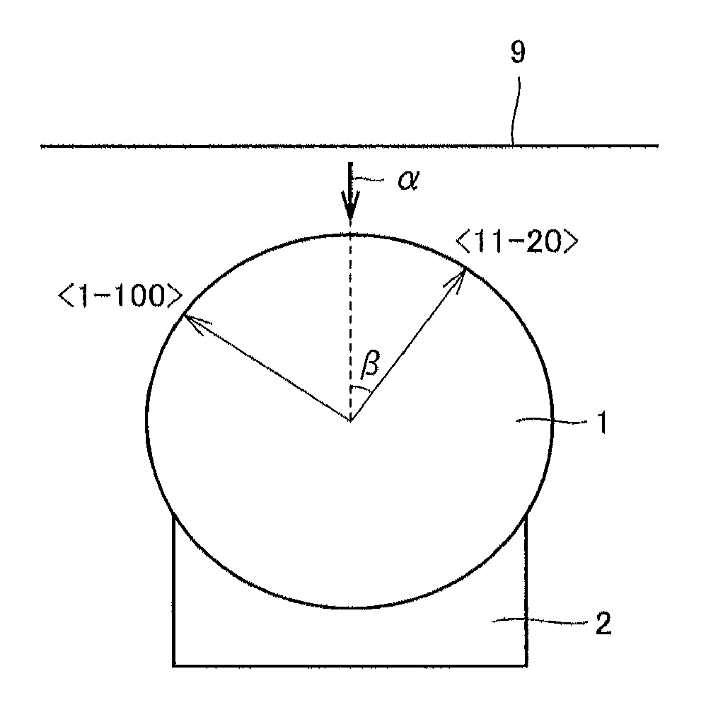
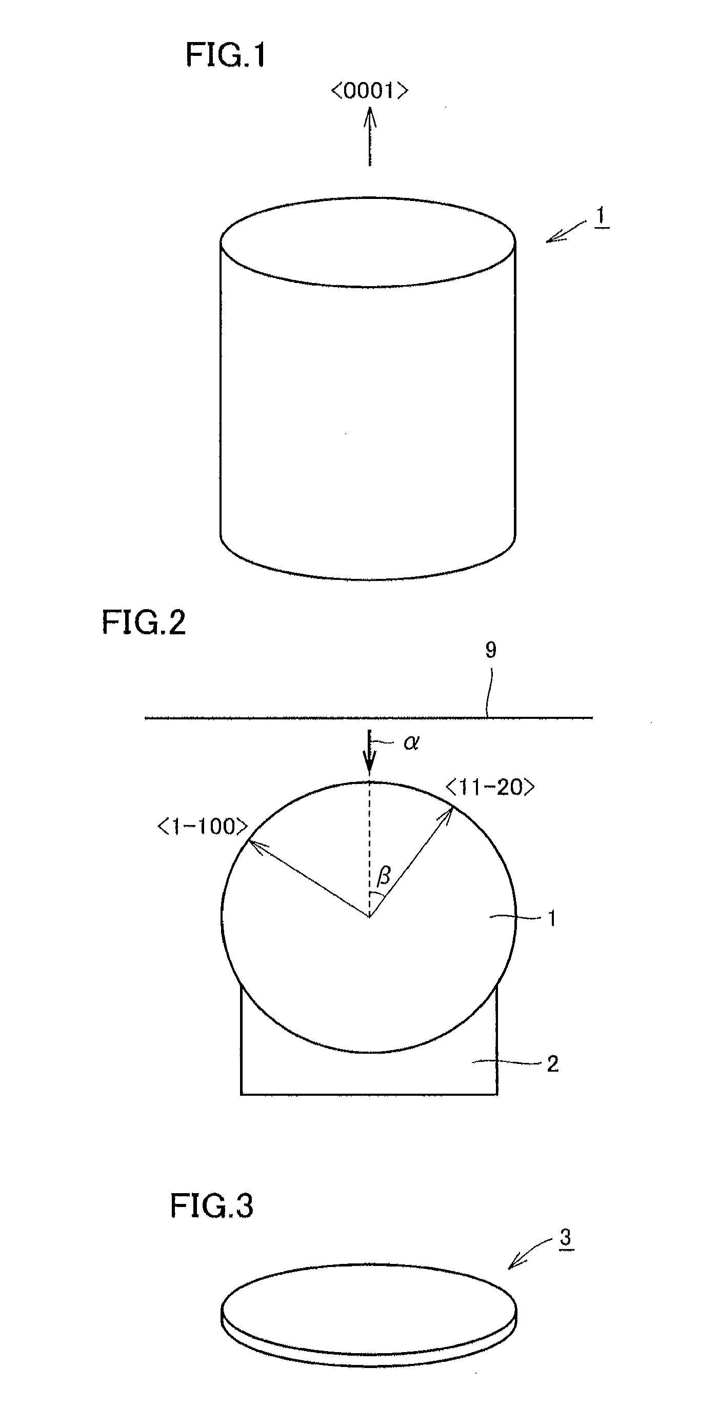
[0051]An experiment for examining influence on warpage (SORI) of an obtained substrate by an angle formed between a direction in which cutting proceeds and the cleavage direction in an orthogonal projection on the {0001} plane in obtaining a substrate by cutting an ingot of single crystal silicon carbide was conducted.
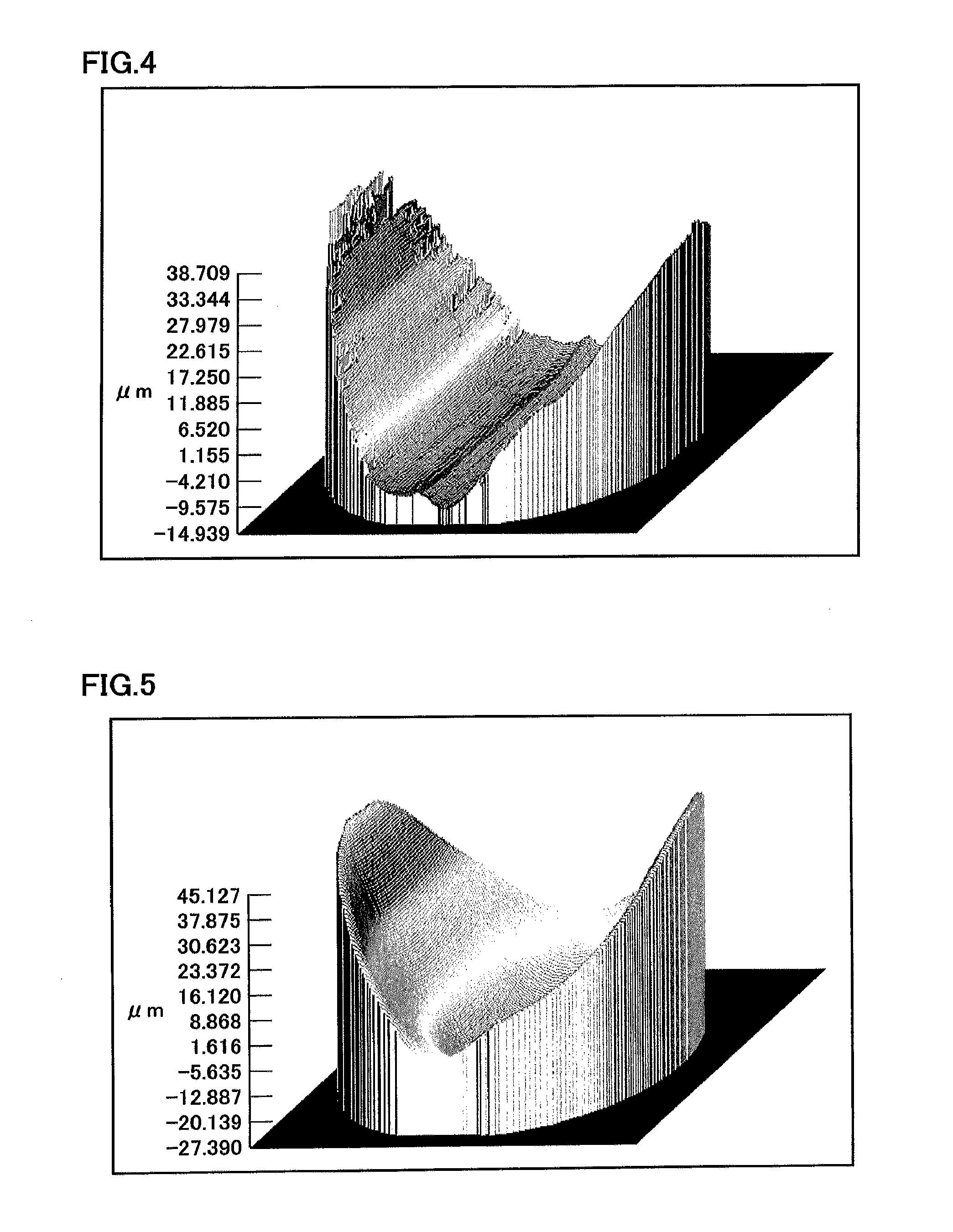
[0052]Initially, as in the embodiment above, an ingot of single crystal silicon carbide was prepared, and a silicon carbide substrate was obtained by slicing the ingot such that an angle formed with respect to the direction representing the cleavage direction was from 0° to 30° in the orthogonal projection on the {0001} plane while the ingot was supported on support base 2. Then, SORI of the main surface of the obtained substrate was measured. Table 1 shows measurement results. In addition, FIGS. 11 to 14 each show a shape of the main surface of the obtained substrate.
TABLE 1Angle Between Direction in Which CuttingProceeds and Direction (°)0101315172030SORI (μm)39261...
PUM
| Property | Measurement | Unit |
|---|---|---|
| Angle | aaaaa | aaaaa |
| Angle | aaaaa | aaaaa |
| Angle | aaaaa | aaaaa |
Abstract
Description
Claims
Application Information