Semiconductor device, and manufacturing method for same

Active Publication Date: 2012-12-06
SHARP KK
View PDF6 Cites 14 Cited by
  • Summary
  • Abstract
  • Description
  • Claims
  • Application Information

AI Technical Summary

Benefits of technology

[0054]According to the present invention, in the semiconductor device provided with an n-type TFT and a p-type TFT, the influence of a parasitic transistor generated in the n-type TFT on the TFT characteristics can be suppressed without actualizing the influence of a parasitic transistor generated in the p-type TFT on the TFT characteristics. Thus, the threshold voltages of the respective TFT

Problems solved by technology

However, if such adjustment is performed, the threshold voltage Vth is also shifte

Method used


Image

  • Semiconductor device, and manufacturing method for same
  • Semiconductor device, and manufacturing method for same
  • Semiconductor device, and manufacturing method for same

Examples


Example

First Embodiment

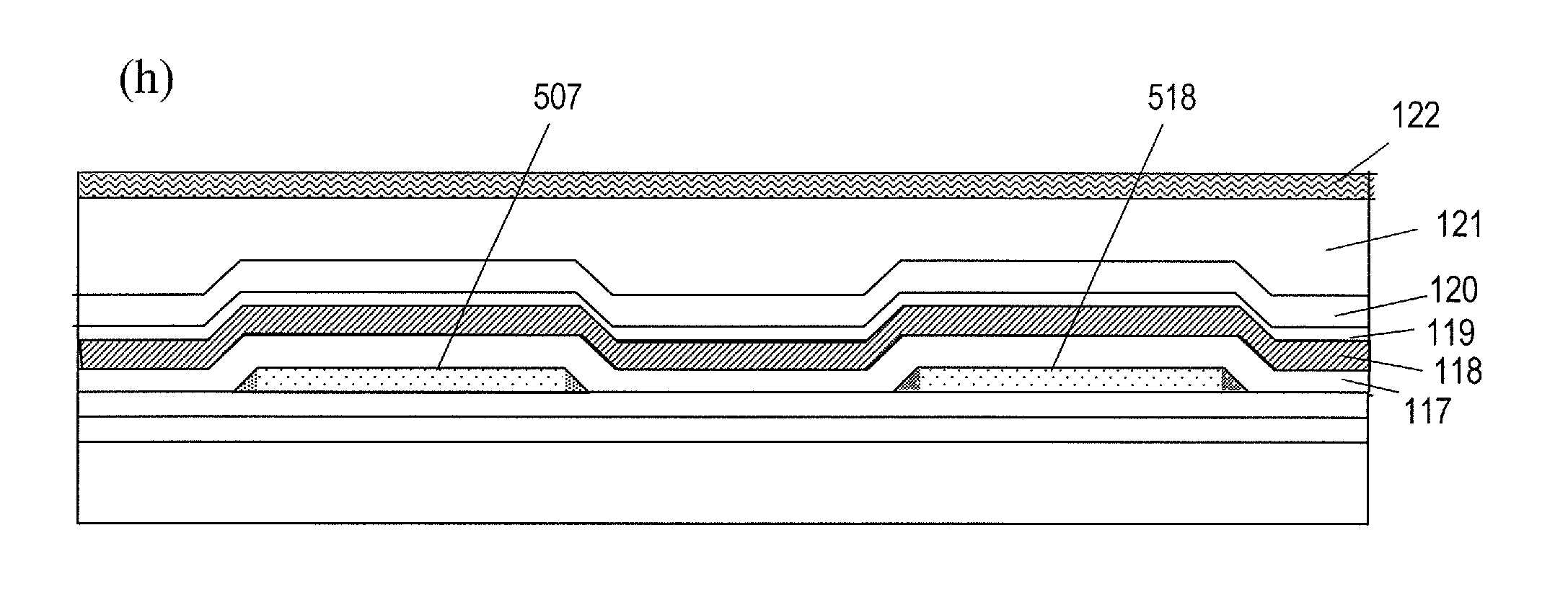
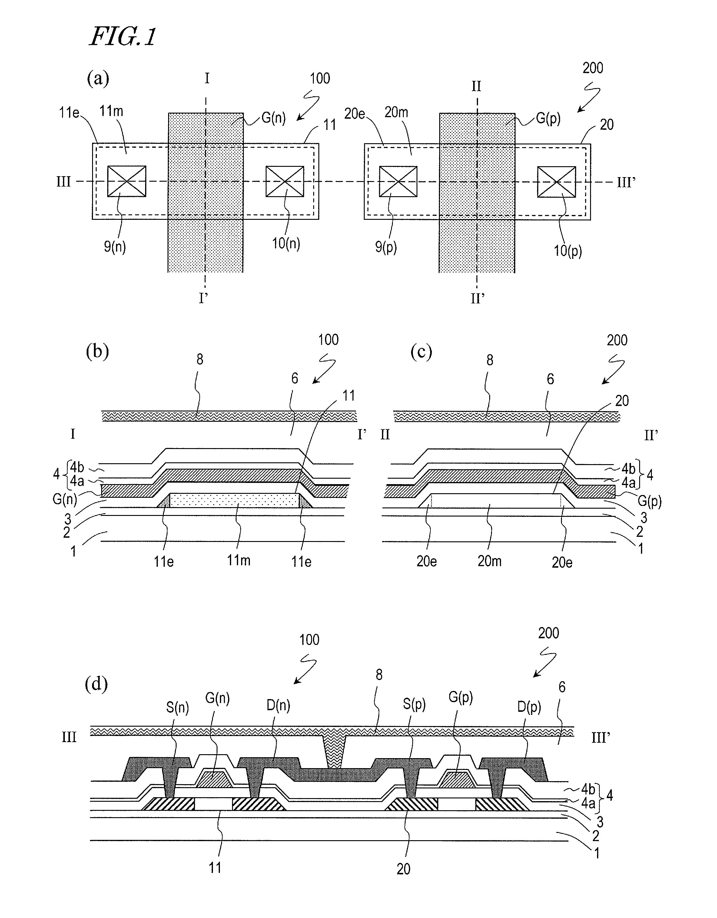
[0113]Hereinafter a semiconductor device in a first embodiment of the present invention will be described with reference to the drawings. The semiconductor device in this embodiment is applied to a substrate provided with a CMOS, e.g., an active matrix substrate provided with a driving circuit including a CMOS. Alternatively, the semiconductor device in this embodiment may be applied to an active matrix substrate in a display device in which a memory circuit including an n-type TFT and a p-type TFT is provided for each pixel.

[0114]FIG. 1(a) is a plan view schematically showing an n-type TFT and a p-type TFT in the semiconductor device of this embodiment. FIG. 1(b) and FIG. 1(c) are cross-sectional views taken along line I-I′ and line II-II′ shown in the plan view of FIG. 1(a), respectively. FIG. 1(d) is a cross-sectional view taken along line III-III′ shown in the plan view of FIG. 1(a). The line I-I′ and the line II-II′ are perpendicular to the channel direction, an...

Example

Second Embodiment

[0165]A semiconductor device in a second embodiment of the present invention will be described. The semiconductor device in this embodiment has the same configuration as that of the semiconductor device in the first embodiment described above with reference to FIG. 1. In addition, similarly to the first embodiment, to a portion of the slope portion of the n-type TFT which is capable of operating at least as a parasitic transistor, a p-type impurity is introduced with the density higher than the main portion of the n-type TFT.

[0166]The present invention and the first embodiment are different in the production methods thereof. Specifically, in the first embodiment, the patterning of the semiconductor layer of the p-type TFT is performed by two etching steps. In the present invention, the patterning of the semiconductor layer of the n-type TFT is performed by two etching steps. Accordingly, the doping condition of the p-type impurity in the slope portion of the respect...

Example

Third Embodiment

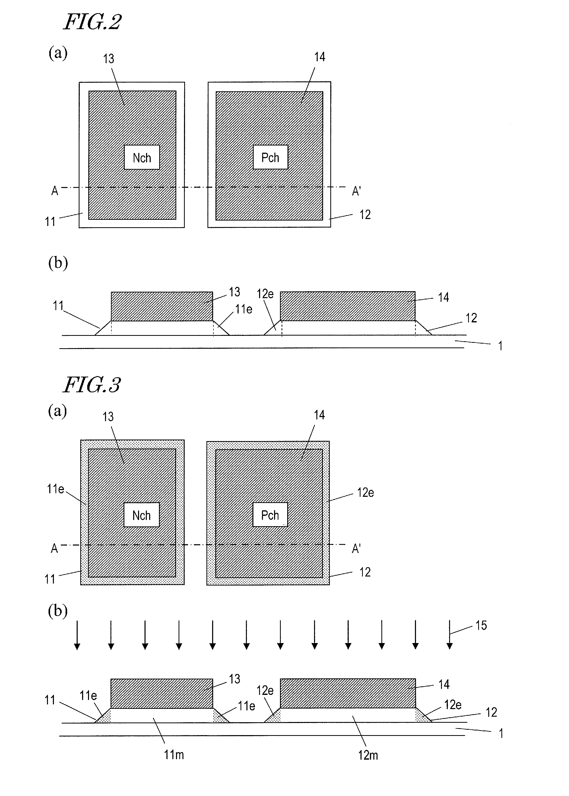
[0195]A semiconductor device in a third embodiment of the present invention will be described. This embodiment is different from the above-described embodiments in that the semiconductor layers of the n-type and p-type TFTs have patterns in which the channel width is smaller than the width of the source and drain regions (so-called “dog-bone pattern”).

[0196]In the above-described embodiments, the island-like semiconductor layers which will act as the active layers of the n-type and p-type TFT have rectangular patterns. However, in the actual circuit, especially in a memory circuit such as an SRAM circuit or a DRAM circuit included in the pixel, an island-like semiconductor layer having a pattern with a small channel width is often used. In such a case, in the island-like semiconductor layer, the width of a channel region (the channel width W) is smaller than the width of a region for forming a contact hole in the channel width direction. That is, the pattern of the s...


PUM


Abstract

A semiconductor device of the present invention includes an n-channel first thin film transistor and a p-channel second thin film transistor on one and the same substrate. The first thin film transistor has a first semiconductor layer (27), and the second thin film transistor has a second semiconductor layer (22). The first semiconductor layer (27) and the second semiconductor layer (22) are formed from one and the same film. Each of the first semiconductor layer (27) and the second semiconductor layer (22) has a slope portion (27e, 22e) positioned in the periphery and a main portion (27m, 22m) which is a portion excluding the slope portion. A p-type impurity is introduced into only a part of the slope portion (27e) of the first semiconductor layer with higher density than the main portion (27m) of the first semiconductor layer, the main portion (22m) of the second semiconductor layer, and the slope portion (22e) of the second semiconductor layer. Accordingly, a driving voltage of the semiconductor device provided with the n-type TFT and the p-type TFT can be reduced.

Description

TECHNICAL FIELD[0001]The present invention relates to a semiconductor device provided with a thin film transistor (Thin Film Transistor: TFT), and a production method thereof.BACKGROUND ART[0002]The development of a semiconductor device in which p-channel and n-channel thin film transistors (TFTs) are formed on one and the same substrate and electronic equipment including such a semiconductor device is promoted.[0003]For example, in an active matrix liquid crystal display device or an organic EL display device, a technique in which a driving circuit is integrally formed on an active matrix substrate is suggested. For the driving circuit, a CMOS (Complementary Metal Oxide Semiconductor) including a p-channel TFT (hereinafter abbreviated as “a p-type TFT”) and an n-channel TFT (hereinafter abbreviated as “an n-type TFT” is employed. In the case where the CMOS is employed, in order to prevent leakage current from occurring, it is necessary to adjust the driving voltage for each TFT in ...

Claims


Application Information

Patent Timeline
IPC IPC(8): H01L29/786H01L21/8238H01L21/336
CPCH01L27/1222H01L27/1288H01L27/092H01L29/78696H01L27/1214H01L27/1277H01L29/045H01L27/1108H10B10/125
Inventor MAKITA, NAOKIMORI, HIROKISAITOH, MASAKI
Owner SHARP KK
Why Eureka
Try Eureka