Direct Coupled Biasing Circuit for High Frequency Applications

a biasing circuit and high frequency technology, applied in pulse generators, instruments, pulse techniques, etc., can solve the problems of introducing undesired and unavoidable parasitic capacitance to ground, power and die (substrates), reducing efficiency, and increasing the power dissipation of the “ac coupling” approach. , to achieve the effect of accurately controlling the power drive characteristics of the next stage, minimizing the distance between stages, and avoiding wasteful die area

Active Publication Date: 2012-12-20
TENSORCOM
View PDF9 Cites 11 Cited by
  • Summary
  • Abstract
  • Description
  • Claims
  • Application Information

AI Technical Summary

Benefits of technology

[0007]In accordance with one aspect of the invention, a resonant circuit is used to isolate a biasing signal from a high frequency signal. The introduction of this resonant circuit in series with the power or ground leads, allows a first stage to be “directly coupled” to a next stage using a metallic trace. The “direct coupling” approach overcomes the wasteful use of die area as described previously for the “AC coupling” or “transformer coupling” approaches used in the high frequency (˜60 GHz) circuit designs since neither capacitors nor transformers are required to transfer the signals between stages. This “direct coupling” invention minimizes the distance between stages by directly coupling and transferring a biasing signal from the first stage to the next stage over the metallic trace connecting these points. In addition, a high frequency signal is also transferred from the first stage to the next stage over the same metallic trace. In the first stage, a resonant circuit in the power supply lead is used to isolate a biasing signal from the high frequency signal. The resonant circuit passes the biasing signal unto the metallic trace carrying the high frequency signal but blocks the high frequency (˜60 GHz) signals on the metallic trace from affecting the biasing signal. This biasing signal is used to accurately control the power drive characteristics of the next stage.

Problems solved by technology

Forming this capacitor on an integrated circuit also introduces an undesired and unavoidable parasitic capacitance to ground, power and die (substrate).
This reduces the efficiency and increases the power dissipation of the “AC coupling” approach.
However, transformers suffer skin loss, coupling loss and die (or substrate) loss.
This increases the power dissipation of this approach since there are twice the stages over that of the “AC coupling” approach.
This reduces the efficiency and increases the power dissipation of the “transformer coupling” approach.
One of the disadvantages of the coupling capacitor and coupling transformer methods is their very large physical size, which translate to larger die area and increased cost.
In addition to these disadvantages, CMOS foundries typically do not provide models or guarantee that the coupling capacitor and transformer modeling for circuits operating more than 20 GHz.
This presents a very significant challenge and difficulties to companies without a modeling group and high frequency measuring equipment.
The additional time needed to perform this analysis increases the length of time to generate the final mask levels for the given technology (known as “tapeout”) and opens the potential for lost revenue.

Method used


Image

  • Direct Coupled Biasing Circuit for High Frequency Applications
  • Direct Coupled Biasing Circuit for High Frequency Applications
  • Direct Coupled Biasing Circuit for High Frequency Applications

Examples


Embodiment Construction

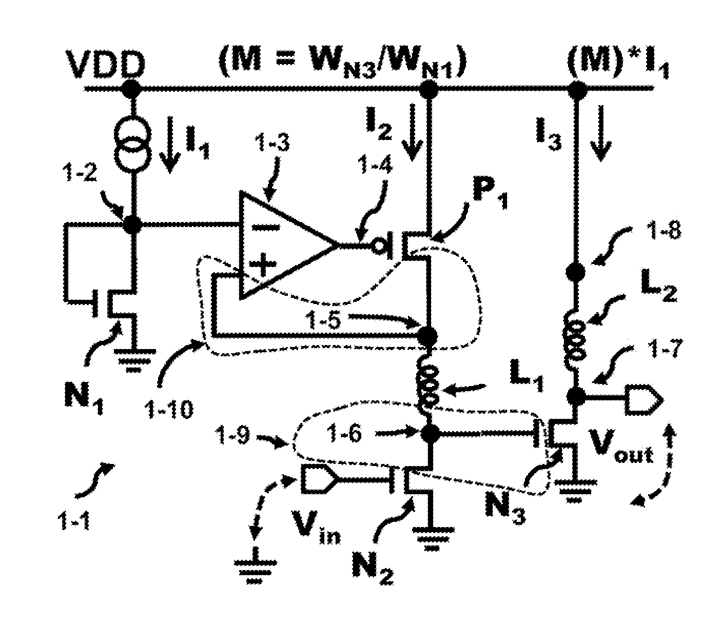
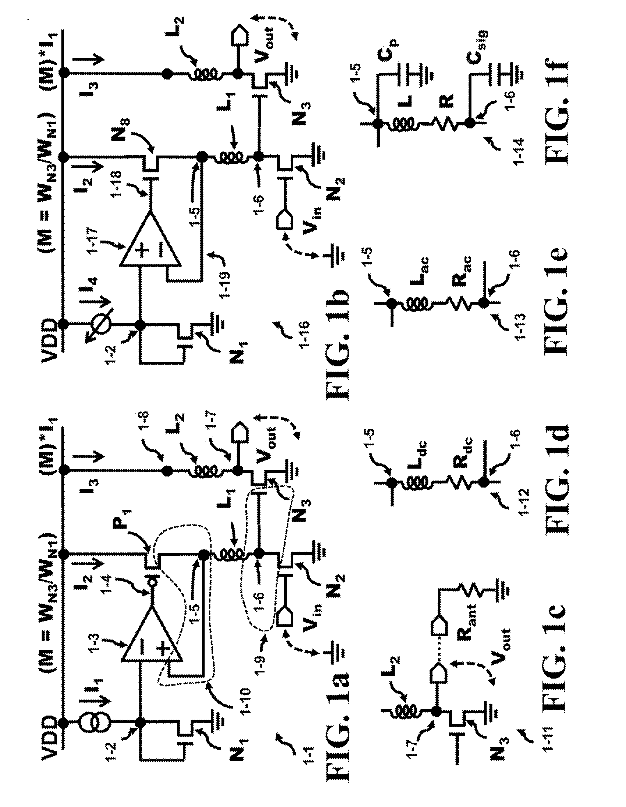
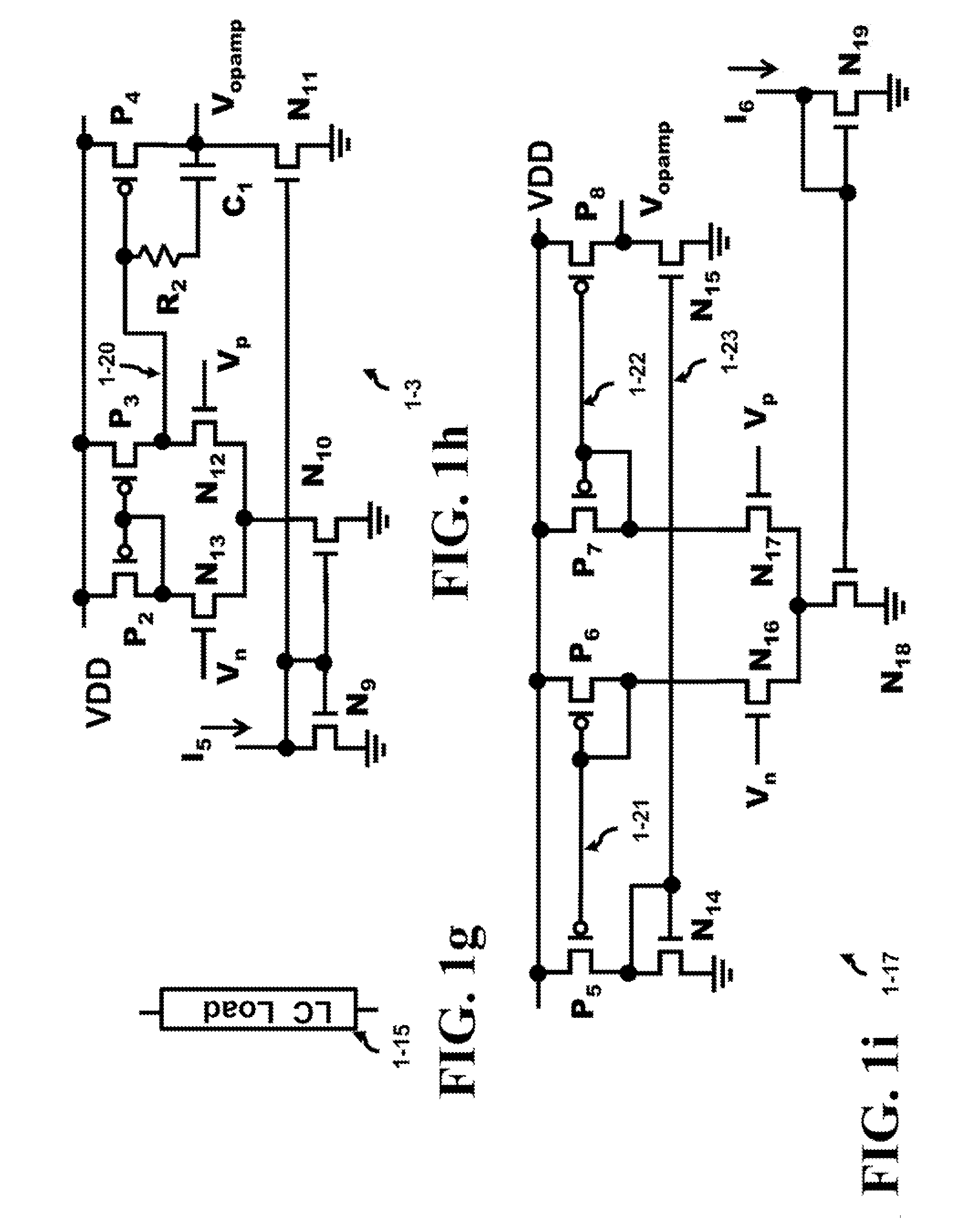
[0024]This invention has been incorporated into a Power Stage (PA) design for a 60 GHz wireless system. The inventive apparatus is applicable to any high frequency system, for example, where the parasitic inductance of a metallic trace is of the order 1 pH per micrometer. At 60 GHz, the typical inductance within or between stages is on the order of about 50 to 120 pH. The actual dimensions of the capacitor depends on several issues; the type of capacitor, the overall positive reactance in a given stage that requires compensation; and, the physical layout of the capacitor, for example. At these frequencies, as a signal is coupled from the first stage to the next stage, the parasitic capacitance and / or the parasitic inductance of the coupling circuits is critical and needs to be minimized. This invention eliminates the need for “capacitor coupling” or “transformer coupling,” and along with them, the associated undesirable parasitic capacitance and inductance. In this invention, the si...


PUM


Abstract

This invention eliminates the need for “capacitor coupling” or “transformer coupling,” and the associated undesirable parasitic capacitance and inductance associated with these coupling techniques when designing high frequency (˜60 GHz) circuits. At this frequency, the distance between two adjacent stages needs to be minimized. A resonant circuit in series with the power or ground leads is used to isolate a biasing signal from a high frequency signal. The introduction of this resonant circuit allows a first stage to be “directly coupled” to a next stage using a metallic trace. The “direct coupling” technique passes both the high frequency signal and the biasing voltage to the next stage. The “direct coupling” approach overcomes the large die area usage when compared to either the “AC coupling” or “transformer coupling” approach since neither capacitors nor transformers are required to transfer the high frequency signals between stages.

Description

BACKGROUND OF THE INVENTION[0001]The Federal Communications Commission (FCC) has allotted a spectrum of bandwidth in the 60 GHz frequency range (57 to 64 GHz). Integrated circuits, formed in semiconductor die, offer high frequency operation in this millimeter wavelength range of frequencies. Some of these integrated circuits utilize Complementary Metal Oxide Semiconductor (CMOS) or Silicon-Germanium (SiGe) technology to form the dice in these designs. At 60 GHz, short on-chip metallic traces translate to inductance values that impact the design of these high frequency circuits. The approximate parasitic inductance of metallic trace in an integrated circuit at this frequency is of the order of 1 pH per micrometer of trace length (2-4 um trace width and 0.85-3 um thickness). At 60 GHz, a typical inductor has an inductance on the order of about 50 to 120 pH and, for one example case, occupies a die area of about 100 um on a side[0002]At these high frequencies (˜60 GHz), there are essen...

Claims


Application Information

Patent Timeline
Patent Type & Authority Applications(United States)
IPC IPC(8): G05F3/02
CPCH04B5/0075G05F3/16H03K17/56H03F3/193H03F3/245H03F1/30H03F2200/555H03F1/56H03F3/195H03F2200/24H03F2200/18H03F2200/12H03K3/012H01Q1/50
Inventor THAM, KHONGMENGSOE, ZAW
Owner TENSORCOM
Why Eureka
Try Eureka