Memory structure and fabricating method thereof

a technology of memory structure and fabrication method, applied in the field of memory structure, can solve problems such as affecting the reliability of devices, erroneous reading, and source region and drain region failing to block secondary

Active Publication Date: 2012-12-27
MACRONIX INT CO LTD
View PDF35 Cites 1 Cited by
  • Summary
  • Abstract
  • Description
  • Claims
  • Application Information

AI Technical Summary

Benefits of technology

[0008]Accordingly, an embodiment of the invention provides a memory structure capable of solving the reading error caused by the second bit effect.
[0009]Another embodiment of the invention provides a method of fabricating a memory structure capable of reducing the programming disturbance caused by secondary hot electrode.
[0030]In light of the foregoing, in the memory structure disclosed in one embodiment of the invention, as at least one of the first charge storage structure and the second charge storage structure includes two charge storage units which are physically separated, the reading error caused by the second bit effect can be prevented and the programming disturbance led by the secondary hot electrode can be reduced.
[0031]Moreover, another embodiment of the invention disclosed a fabricating method of a memory structure which can be integrated with the conventional fabrication. As a consequence, the fabrication complexity is decreased effectively.

Problems solved by technology

However, when defects are present in a tunnel oxide layer disposed under the polysilicon floating gate, current leakage of devices then occurs easily, thereby affecting the reliability of devices.
As the miniaturization of the gate length leads to the approximation of two charge storage units located on the left and right in the same memory cell, a severe second bit effect then occurs and easily results in erroneous reading.
In addition, since the source region and the drain region are miniaturized, the source region and the drain region fail to block the secondary hot electrons generated when the selected memory cell is programmed.
The second hot electrode is thus injected into the adjacent memory cell to generate program disturbance and thereby lowering the reliability of memory device.

Method used


Image

  • Memory structure and fabricating method thereof
  • Memory structure and fabricating method thereof
  • Memory structure and fabricating method thereof

Examples


first embodiment

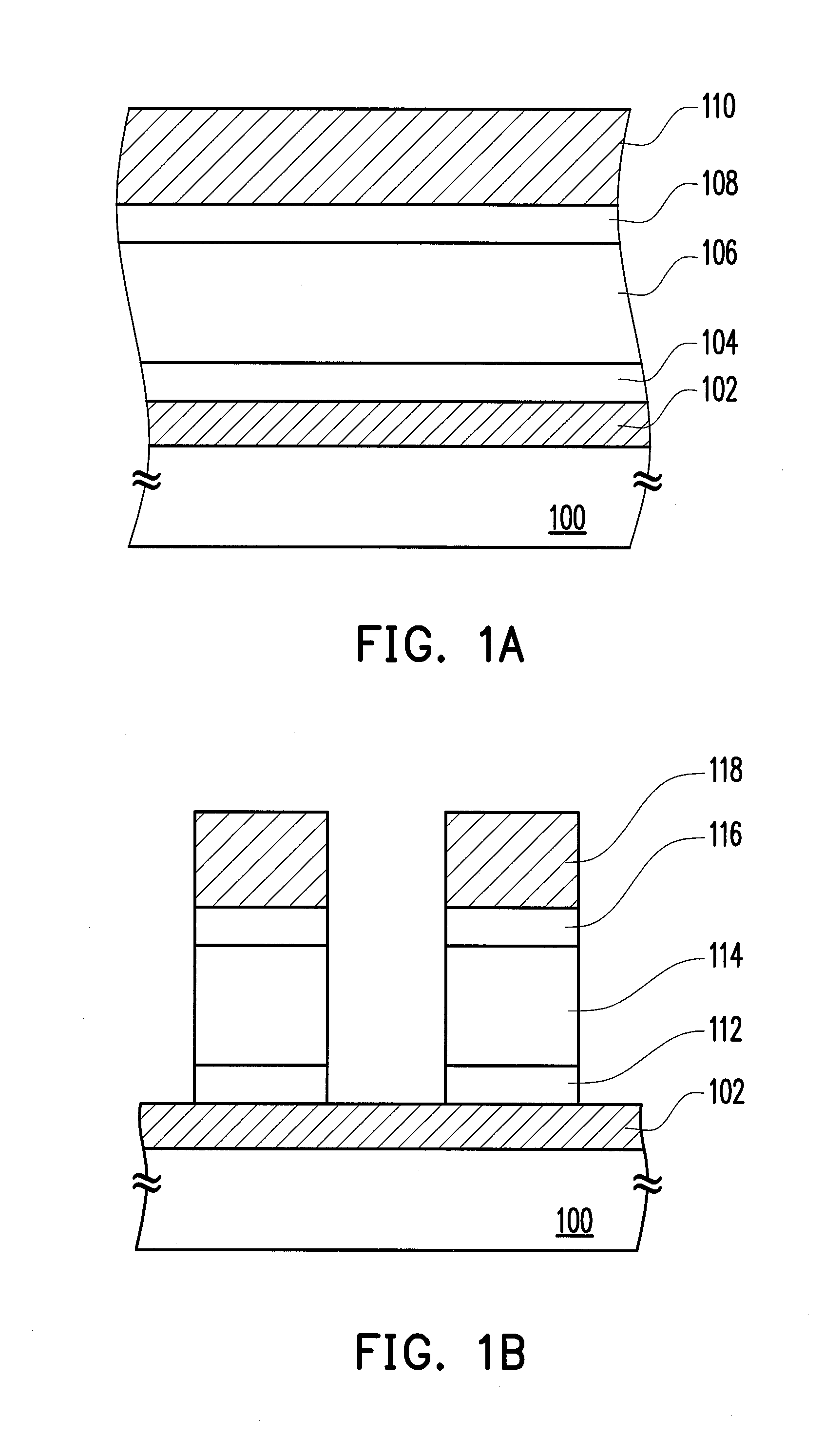
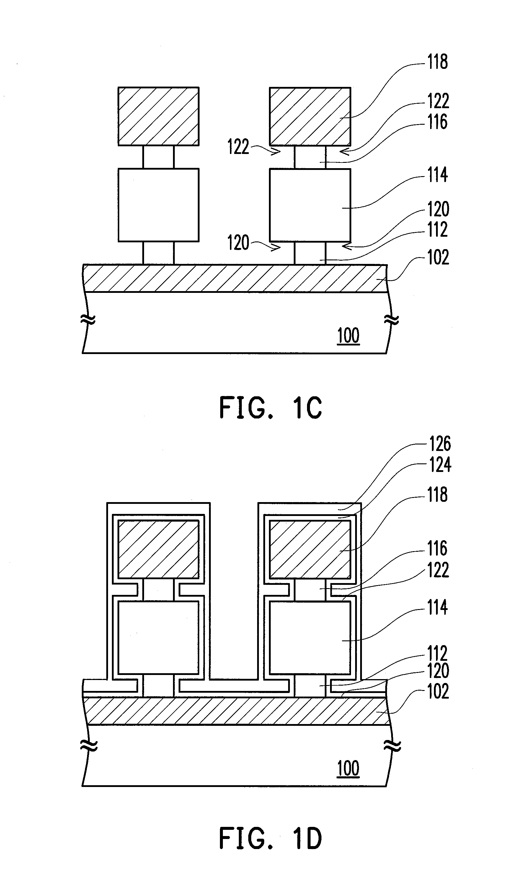
[0038]FIGS. 1A to 1H are cross-sectional diagrams illustrating a flow chart for fabricating a memory structure according to the invention.

[0039]Referring to FIG. 1A, a gate 102 is first formed on a substrate 100. The gate 102 is, for example, an N-type doped region and the substrate 100 is, for example, a P-type doped substrate. The N-type gate 102 and the P-type substrate 100 have contrary doping types and can therefore block charges from communicating therebetween. In another embodiment, the substrate 100 can also be a P-type well region (not shown) located in an N-type well region (not shown), so that the gate 102 is formed on the P-type well region on the substrate 100. When the gate 102 is the N-type doped region, a method of forming the gate 102 includes implanting a dopant in the substrate 100 using an ion implantation method, for instance.

[0040]In another embodiment, the gate 102 is a doped polysilicon gate. When the gate 102 is a doped polysilicon gate, an isolation dielect...

fourth embodiment

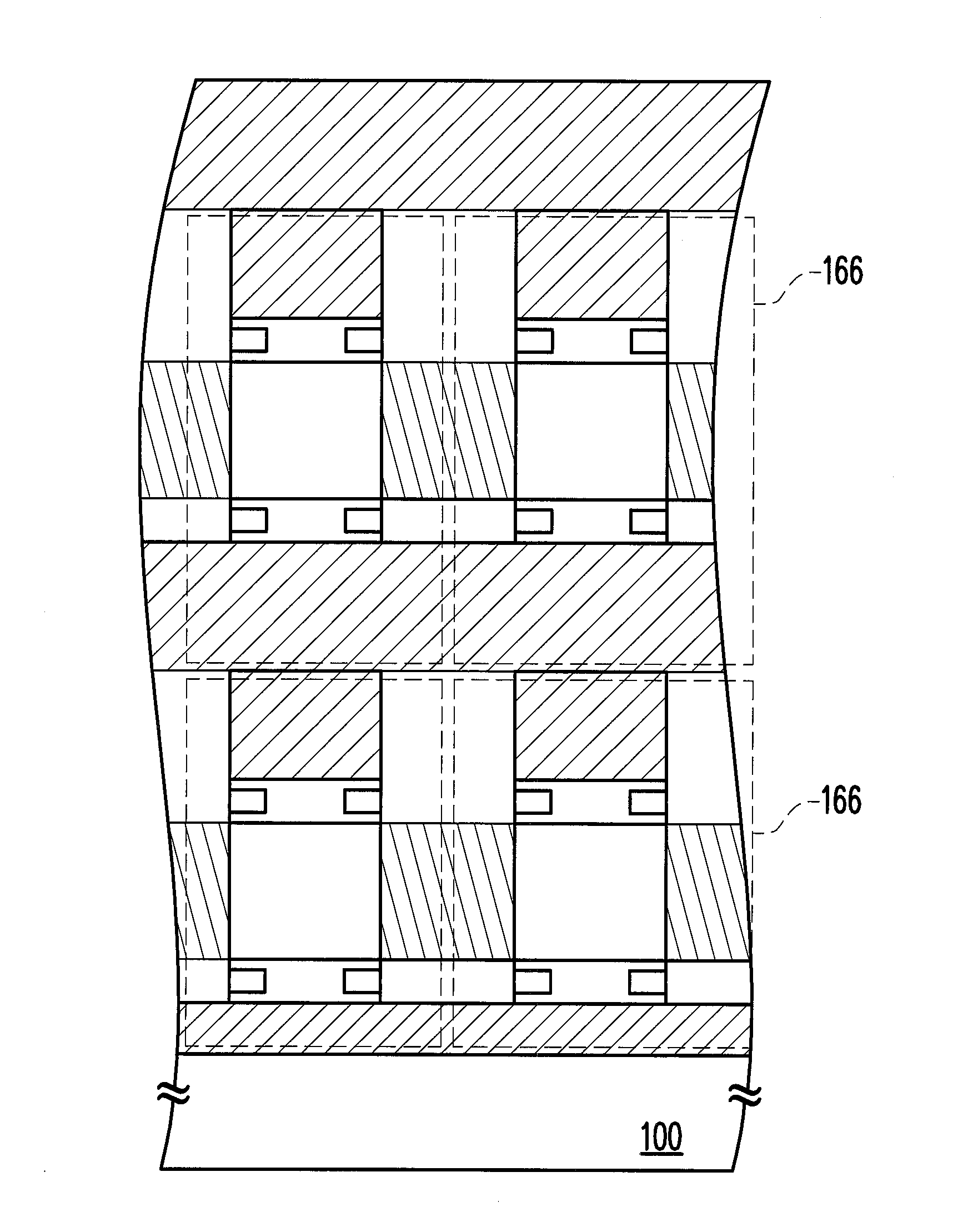
[0070]FIG. 5 illustrates a cross-sectional view of a memory structure according to the invention.

[0071]The difference between the memory structures in the first embodiment and the fourth embodiment is that the memory structure in the fourth embodiment has a plurality of memory cells 166 stacked together, where every two memory cells 166 that are perpendicularly adjacent to each other share a common word line. Other elements in the fourth embodiment are similar to those in the first embodiment and the descriptions are thus omitted hereinafter.

[0072]In the fourth embodiment, since the memory structure has a plurality of memory cells 166 which is stacked together, the integrity of the memory device can further be increased.

[0073]In summary, the embodiments aforementioned include at least the following advantages.

[0074]The memory structure provided in the embodiments aforementioned is capable of solving the reading error caused by the second bit effect and reducing the programming distu...


PUM


Abstract

A memory structure including a memory cell is provided, and the memory cell includes following elements. A first gate is disposed on a substrate. A stacked structure includes a first dielectric structure, a channel layer, a second dielectric structure and a second gate disposed on the first gate, a first charge storage structure disposed in the first dielectric structure and a second charge storage structure disposed in the second dielectric structure. At least one of the first charge storage structure and the second charge storage structure includes two charge storage units which are physically separated. A first dielectric layer is disposed on the first gate at two sides of the stacked structure. A first source and drain and a second source and drain are disposed on the first dielectric layer and located at two sides of the channel layer.

Description

BACKGROUND OF THE INVENTION[0001]1. Field of the Invention[0002]The invention related to a memory structure and a fabricating method thereof. More particularly, the invention relates to a memory structure having a plurality of charge storage units which is physically separated and a fabricating method thereof[0003]2. Description of Related Art[0004]A memory is a semiconductor device designed to store information or data. As micro-processors become more functional, the programs and operations performed by software increase as well. Thus, the demand for high capacity memory becomes higher. In various memory products, non-volatile memory such as electrically erasable programmable read only memory (EEPROM) allows multiple data programming, reading, and erasing operations. Here, the data stored therein are saved even after the memory has been disconnected. According to the advantages mentioned above, EEPROM has become a memory widely adopted in personal computers and electronic apparatus...

Claims


Application Information

Patent Timeline
Patent Type & Authority Applications(United States)
IPC IPC(8): H01L29/792H01L21/336
CPCH01L29/7887H01L29/7923H01L29/792H01L27/11578H01L27/11551H01L29/40114H10B41/20H10B43/20H01L29/42332H01L29/66825
Inventor CHENG, CHENG-HSIENTSAI, WEN-JERYAN, SHIH-GUEICHENG, CHIH-CHIEHHUANG, JYUN-SIANG
Owner MACRONIX INT CO LTD
Why Eureka
Try Eureka