Methods and Devices for Sensing Device Signal Correction
a technology of sensing devices and signals, applied in measurement devices, scientific instruments, instruments, etc., can solve problems such as delay in patient receipt, increase analysis cost of laboratory tests, and adverse to patient condition or prognosis
- Summary
- Abstract
- Description
- Claims
- Application Information
AI Technical Summary
Benefits of technology
Problems solved by technology
Method used
Image
Examples
examples
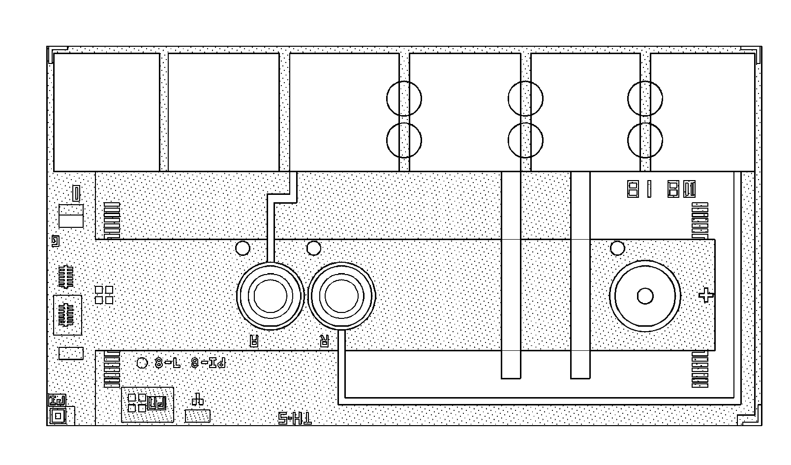
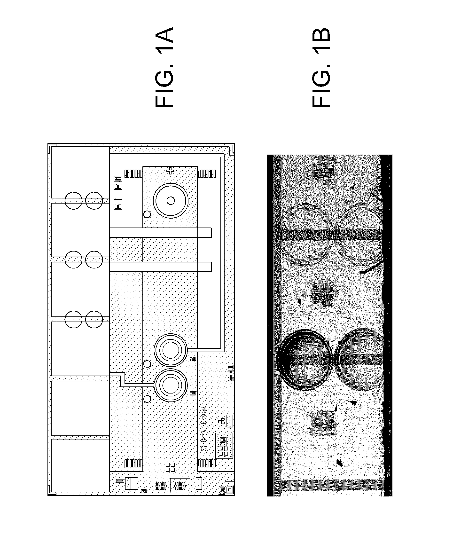
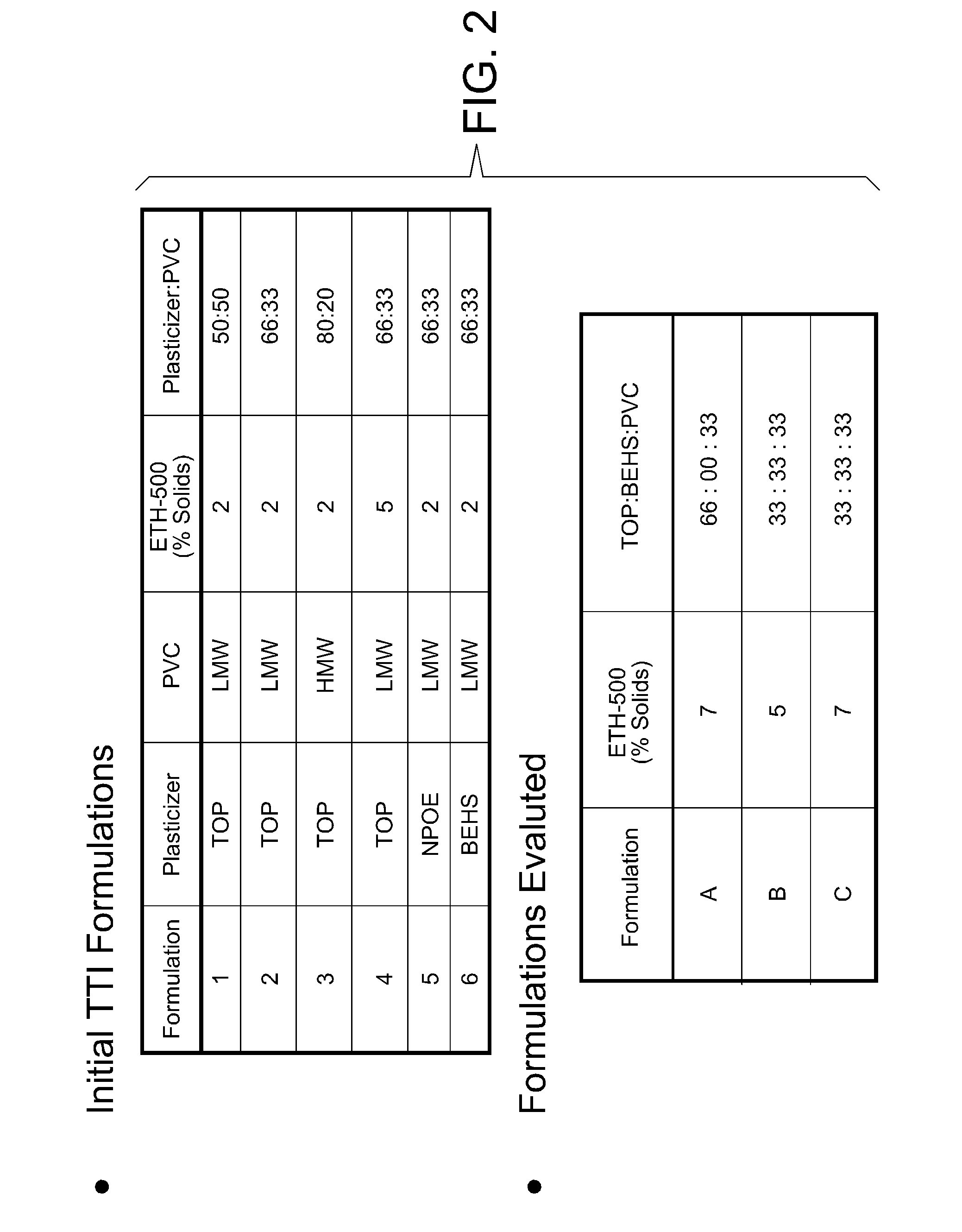
[0059]Six TTI material formulations were tested on silicon chips of the type shown in FIGS. 1A and 1B. The silicon chips were made on wafers according to the general processes as described in jointly owned U.S. Pat. No. 5,200,051 and U.S. Pat. No. 7,419,821. Six contact pads are shown at the top of the chip, two of which are each connected to a round amperometric sensor by a conducting line, and two are connected to parallel hematocrit sensing bars. Six circles indicate the locations for printing the TTI material. The overall dimensions of the chip are about 3×5 mm and the TTI material diameter is about 0.2 mm. FIG. 1B is an image of an actual chip with two rings printed with TTI material (left) and two rings without TTI material (right). Four optional positions for boundary structures are shown. Note the domed shape of the printed structure is apparent in FIG. 1B. The boundary structure may be formed, for example, by patterning a ridge of passivation material, e.g., a photoformable...
PUM
 Abstract
Description
Claims
Application Information


