

Method of fabricating light receiving element and apparatus for fabricating light receiving element
a technology of light receiving element and light receiving element, which is applied in the direction of sustainable manufacturing/processing, final product manufacturing, vacuum evaporation coating, etc., can solve the problem of increasing the burden of fabrication work, limited wavelength range of light to be received, and not focused on how to easily fabricate light receiving element. problem, to achieve the effect of easy fabrication of light receiving elemen
- Summary
- Abstract
- Description
- Claims
- Application Information
AI Technical Summary
Benefits of technology
Problems solved by technology
Method used
Image

Examples
Embodiment Construction
[0021]Hereafter, an embodiment of the invention is described in detail.
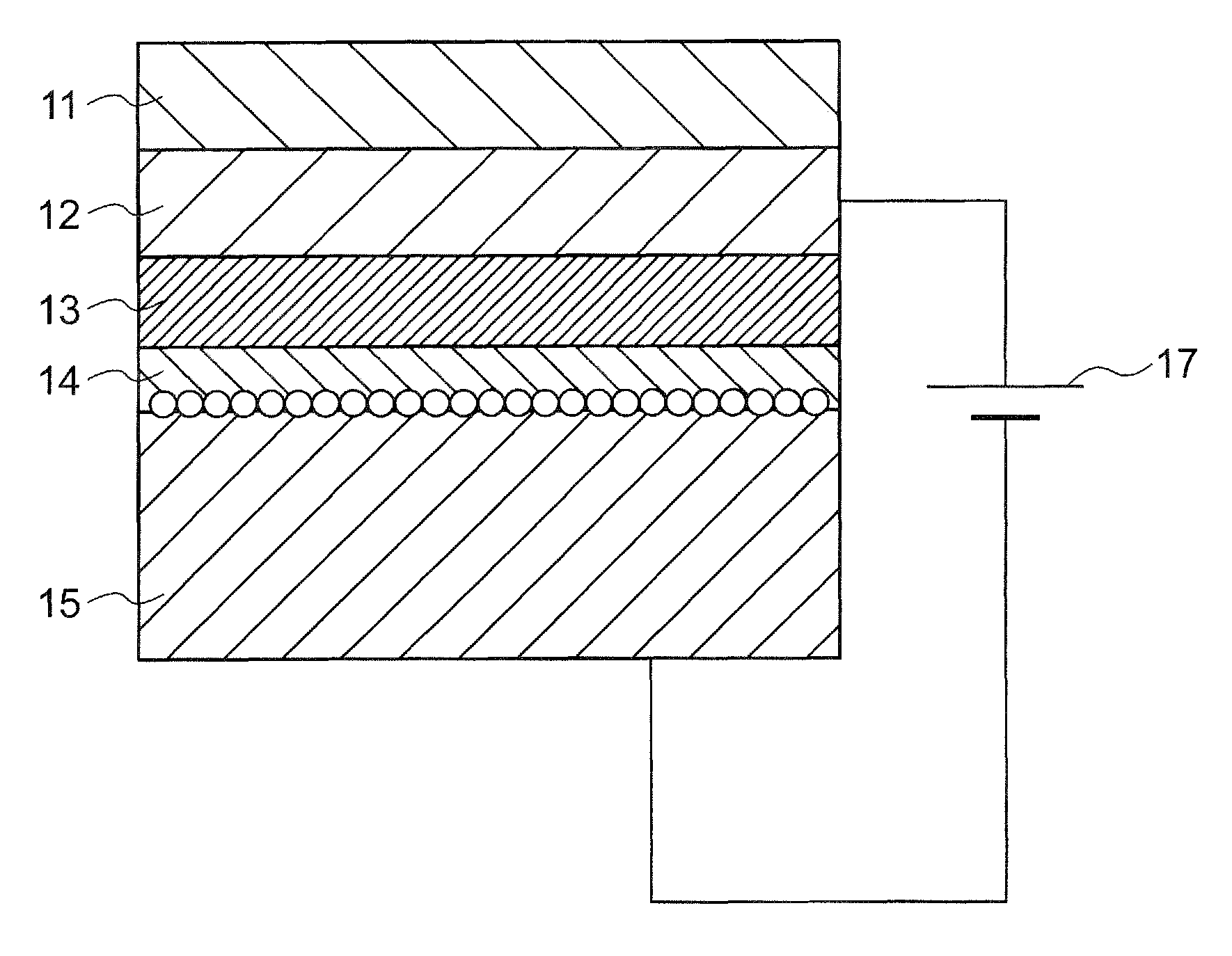
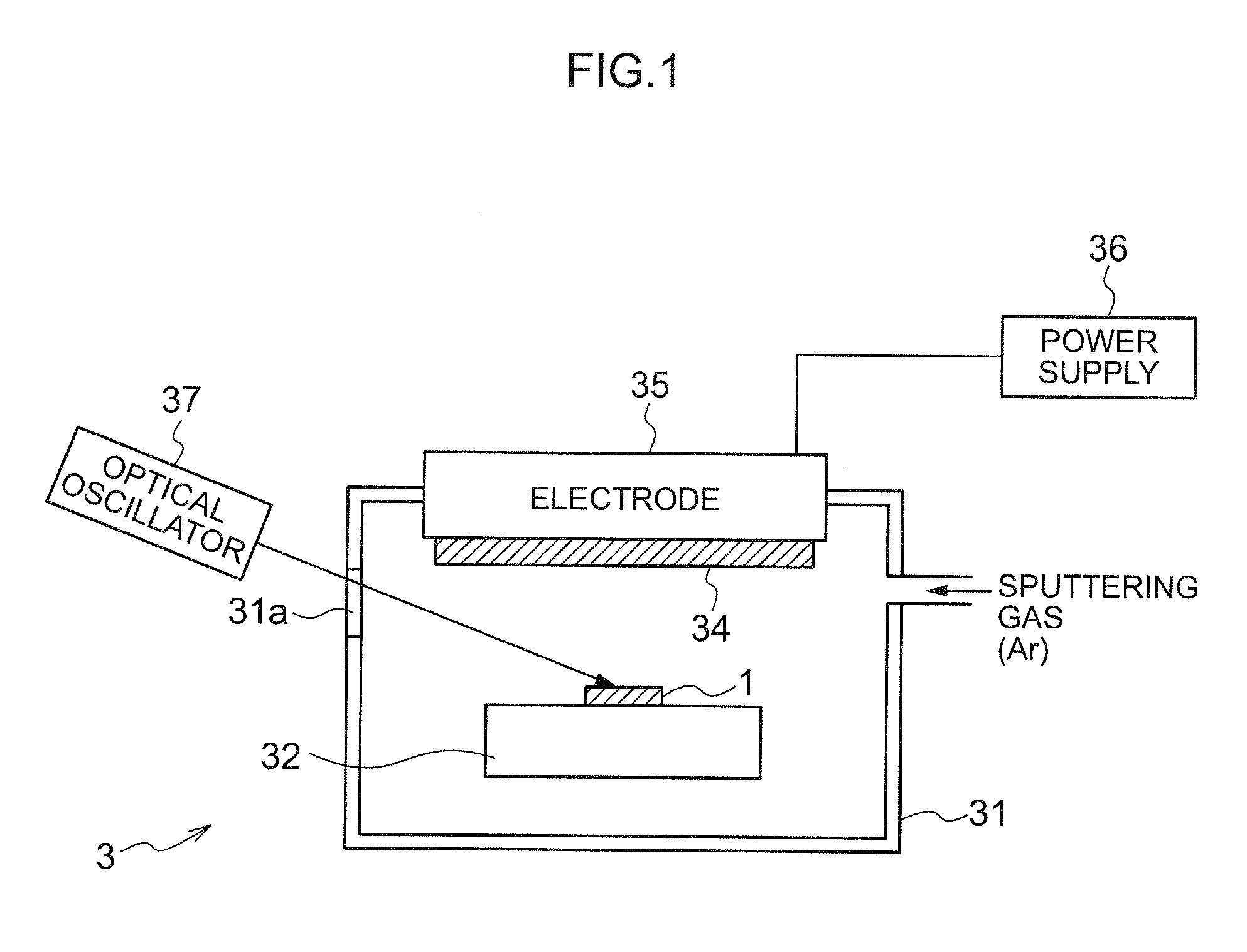
[0022]FIG. 1 shows the configuration of a sputtering system 3 for achieving a method of fabricating a light receiving element to which the invention is applied.
[0023]The sputtering system 3 is configured to include a chamber 31, a table 32 for mounting a light receiving element 1, a target 34 disposed on the opposite side to the light receiving element 1, and an electrode 35 to which the target 34 is attached. The table 32, the target 34 and the electrode 35 are disposed in the chamber 31. The sputtering system 3 further includes, outside the chamber 31, a power supply 36 connected to the electrode 35, and an optical oscillator 37 disposed on a side or the like of the chamber 31.
[0024]In the sputtering system 3, after exhausting the inside of the chamber 31 to about 10−2 Torr, inactive gas, such as Ar, is introduced, and a voltage is applied to the electrode from the power supply 36 to cause discharging. This mak...
PUM
| Property | Measurement | Unit |
|---|---|---|
| wavelength | aaaaa | aaaaa |
| wavelength | aaaaa | aaaaa |
| absorption wavelength | aaaaa | aaaaa |
Abstract
Description
Claims
Application Information