
Metal-oxide films from small molecules for lithographic applications

a technology of metal-oxide films and lithographic applications, which is applied in the direction of photosensitive materials, instruments, photomechanical equipment, etc., can solve the problems of reducing the the inability to achieve sufficient lithographic performance for high-volume manufacturing, and the inability to reduce the thickness of the photoresist. the effect of reducing the thickness

Active Publication Date: 2013-01-10
BREWER SCI
View PDF2 Cites 164 Cited by
  • Summary
  • Abstract
  • Description
  • Claims
  • Application Information

AI Technical Summary

Benefits of technology

The present invention provides a hardmask composition for use in forming microelectronic structures. The composition is substantially free of silicon and comprises a metal-oxide precursor compound dispersed or dissolved in a solvent system. The precursor compound can be selected from the group consisting of polymers, oligomers, monomers, and mixtures thereof. The hardmask composition is insoluble in aqueous alkaline developers and can be used to form a cured hardmask layer on a substrate. The technical effect of the invention is to provide a hardmask composition that can effectively protect the substrate during the formation of microelectronic structures.

Problems solved by technology

However, Rayleigh's law also shows that enhancing resolution causes the DOF to decrease.
However, the reduced photoresist thickness cannot offer sufficient etch resistance to transfer the pattern into the substrate, especially for 193-nm ArF photolithography.
Due to the transparency requirement, aromatic structures cannot be put into ArF resists, so most ArF resists etch even faster than previous photoresists.
One of their drawbacks is the difficulty of obtaining sufficient lithographic performance for high-volume manufacturing.
Unfortunately, almost all currently-available photoresists still etch relatively rapidly under common hardmask plasma etch chemistries, and silicon hardmasks do not provide sufficient etch selectivity for thinner photoresists.
However, undercutting is very difficult to control in an isotropically developable bottom anti-reflective coating.
On the other hand, if they are coated on top of a spin-on carbon, planarization layer, those organic bottom anti-reflective coating materials are not effective as hardmasks.

Method used


Image

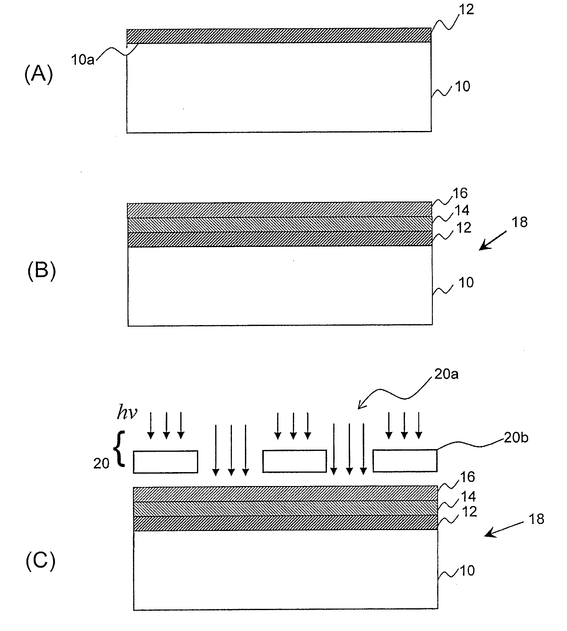
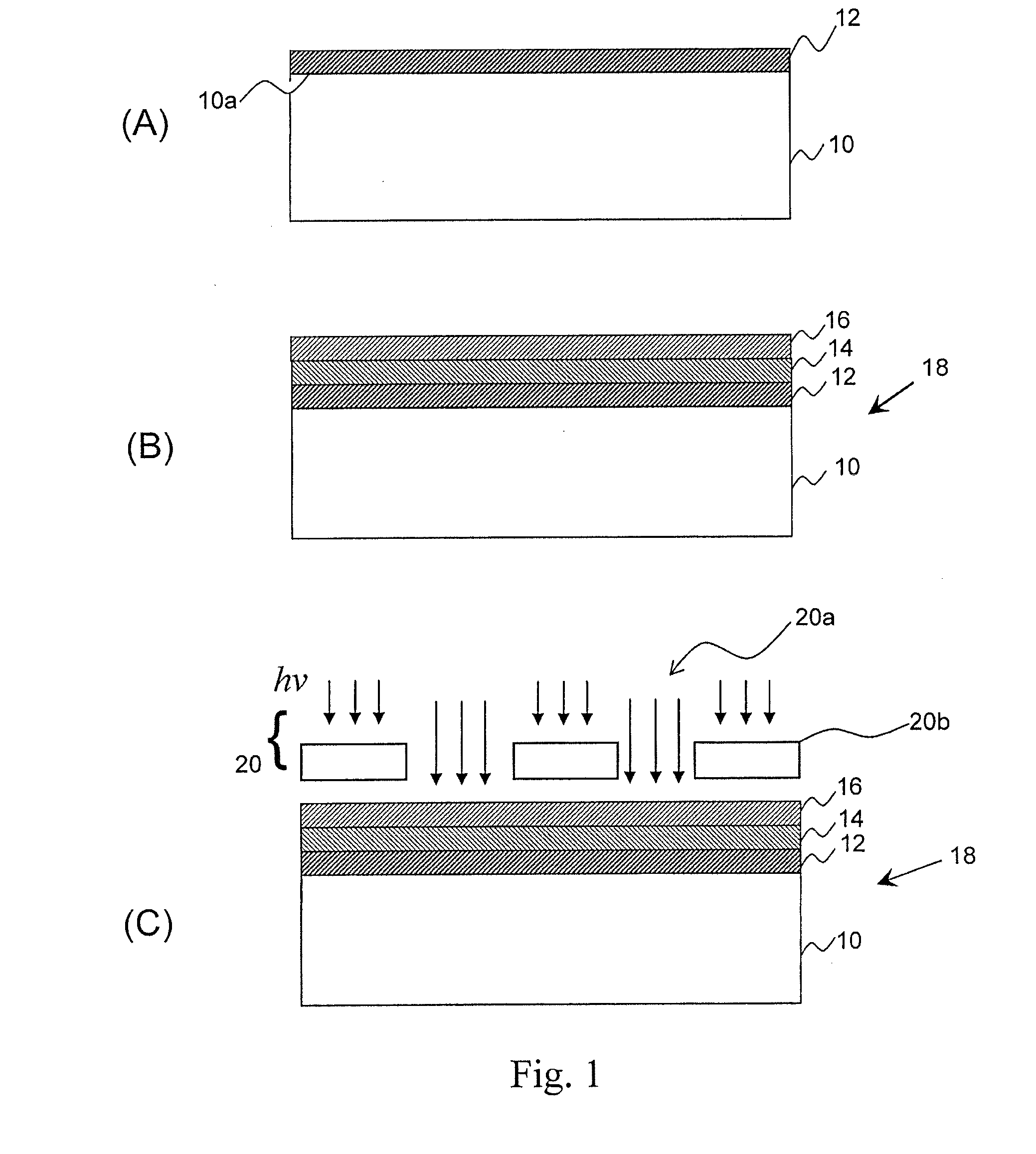
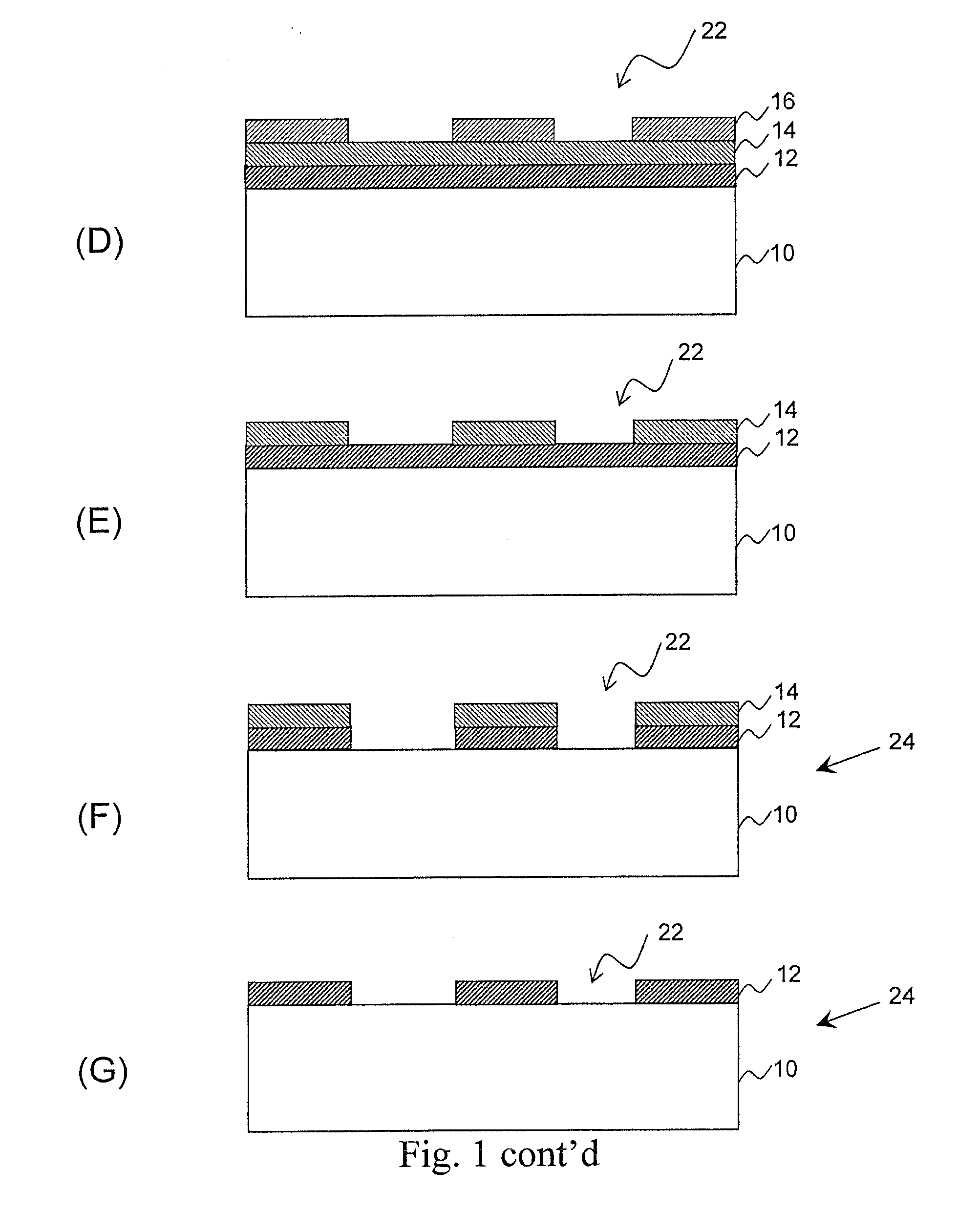
  • Metal-oxide films from small molecules for lithographic applications
  • Metal-oxide films from small molecules for lithographic applications
  • Metal-oxide films from small molecules for lithographic applications

Examples


example 1

Aluminum / Silicon Sol-Gel Hardmask

[0049]1. Polymer Synthesis

[0050]To prepare the polymer, 1.32 grams of phenyl trimethoxysilane (Gelest; Morrisville, Pa.), 6.54 grams of vinyl trimethoxysilane (Gelest), 14.06 grams of methyl trimethoxysilane (Gelest), 45.11 grams of aluminum diisopropoxide ethylacetoacetate (solution of 75% solids in IPA from Gelest, diluted to 40% solids with PGMEA), and 93.00 grams of PGMEA (Ultra Pure Solutions, Inc.) were added to a round-bottom flask. Over a 10-minute period, 17.15 grams of a 3N acetic acid solution (17.6% acetic acid and 82.4% water) were added slowly to the flask while stirring. The round-bottom flask was fitted with a distillation head, distillation column, and collection flask. The solution was then heated at 95° C. for 3 hours.

[0051]2. Hardmask Formulation

[0052]A hardmask formulation was prepared by mixing 12.03 grams of the polymer solution above (˜8.88% solids) with 6.36 grams of PGMEA, 16.4 grams of PGME, and 0.89 grams of a 0.4% solutio...

example 2

Titanium / Silicon Sol-Gel Hardmask

[0055]1. Polymer Synthesis

[0056]In this Example, the polymer was prepared by adding 1.21 grams of phenyl trimethoxysilane (Gelest), 6.00 grams of vinyl trimethoxysilane (Gelest), 11.01 grams of methyl trimethoxysilane (Gelest), 68.06 grams of titanium diisopropoxide (bis 2,4-pentanedione) (solution of 75% solids in IPA from Gelest, diluted to 40% solids with PGMEA), and 80.50 grams of PGMEA (Ultra Pure Solutions, Inc.) to a round-bottom flask. Over a 10-minute period, 17.08 grams of a 3N acetic acid solution (17.6% acetic acid and 82.4% water) were slowly added to the flask while stirring. The round-bottom flask was fitted with a distillation head, distillation column, and collection flask. The solution was then heated at 95° C. for 4 hours.

[0057]2. Hardmask Formulation

[0058]A hardmask formulation was prepared by mixing 6.01 grams of the polymer solution above (9.06% solids) with 17.85 grams of PGMEA, and 12.39 grams of PGME to make a 1.5% solids sol...

example 3

Titanium / Silicon Sol-Gel Hardmask 2

[0061]1. Polymer Synthesis

[0062]In this procedure, as second titanium / silicon sol-gel hardmask was prepared. To synthesize the polymer, 21.11 grams of methyl trimethoxysilane (Gelest), 32.40 grams of titanium diisopropoxide (bis 2,4-pentanedione) (75% solids in IPA, Gelest), and 117.50 grams of PGMEA (Ultra Pure Solutions, Inc.) were added to a round-bottom flask. Over a 10-minute period, 5.75 grams of a 3N acetic acid solution (17.6% acetic acid and 82.4% water) were added slowly to the flask while stirring. The round-bottom flask was fitted with a distillation head, distillation column, and collection flask, and the solution was heated at 95° C. for 4 hours.

[0063]2. Hardmask Formulation

[0064]A hardmask formulation was prepared by mixing 6.00 grams of the polymer solution above (9.56% solids) with 19.03 grams of PGMEA, 3.05 grams of PGME, and 0.72 grams of a 0.4% solution of benzyltriethylamino chloride (BTEAC) in PGME to make a 2.0% solids soluti...


PUM

PropertyMeasurementUnit
sizesaaaaaaaaaa
total weightaaaaaaaaaa
microelectronics structureaaaaaaaaaa

Abstract

Metal-oxide films for lithographic applications are provided. The films are formed from compositions comprising metal-oxide precursor compounds including metals and metalloids other than silicon. These films are easily produced and can be modified with a variety of ligands, including alkoxides, phenoxides, carboxylates, beta-diketones, and beta-ketoesters.

Description

BACKGROUND OF THE INVENTION[0001]1. Field of the Invention[0002]The present invention relates in general to new hardmask compositions having improved etch resistance for use in the manufacture of microelectronics devices. The compositions comprise metal-oxide precursors dispersed or dissolved in a solvent system.[0003]2. Description of Related Art[0004]The advances of microelectronic manufacture are reflected by the density and dimensions of semiconductor structures created by the microphotolithographic process. The demand for high density and small critical dimension (CD) has been constantly pushing photolithography technology to its limits. To keep pace with the semiconductor industry roadmap, next-generation patterning materials and innovative lithographic processes will be needed to work in unison for high-resolution lithography. As critical feature sizes keep shrinking to 32 nm and beyond, and while the aspect ratios of printed lines have certain limits to avoid possible line c...

Claims


Application Information

Patent Timeline
Patent Type & Authority Applications(United States)
IPC IPC(8): B32B3/10B05D3/02G03F7/004C09D183/00G03F7/20
CPCC08G77/58C08J5/00C09D183/14G03F7/0752Y10T428/24802G03F7/091G03F7/094H01L21/0276H01L21/0332G03F7/09
Inventor SULLIVAN, DANIEL M.NEEF, CHARLES J.WANG, YUBAOOUATTARA, TANTIBORO
Owner BREWER SCI
Learn More