Plasma display panel

Inactive Publication Date: 2013-01-17
PANASONIC CORP
View PDF5 Cites 2 Cited by
  • Summary
  • Abstract
  • Description
  • Claims
  • Application Information

AI Technical Summary

Benefits of technology

[0018]In a PDP of one aspect of the present invention having the structure described above, Sr adjusted to a predetermined concentration within the bounds of not increasing an aging time is further included in a protective film containing CeO2. Consequently, in a band structure, a Sr-originated electronic level is formed in a forbidden band, and the position of the upper end of a valence band is elevated, so that electrons in the valence band exist at a relatively shallow level. Therefore, when the PDP is driven, a large amount of electrons existing at an impurity level and around the upper end of the valence band can be involved in electron discharge using energy available in the process of Auger neutralization by Xe atoms of a discharge gas and the like. Using the increased energy, secondary electron emission property of the protective film is considerably improved, so that in the PDP, discharge can be started in high responsivity at a relatively low discharge starting voltage, and the discharge delay can b

Problems solved by technology

An increase in operating voltage i

Method used


Image

  • Plasma display panel
  • Plasma display panel
  • Plasma display panel

Examples


first embodiment

General Structure of PDP 1

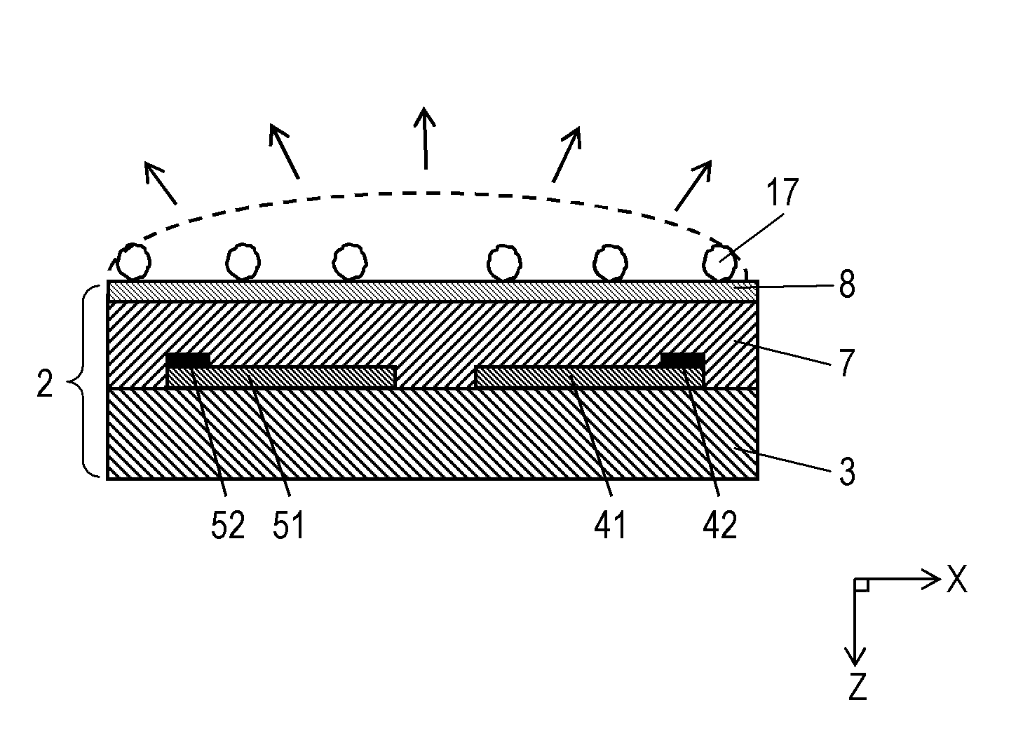
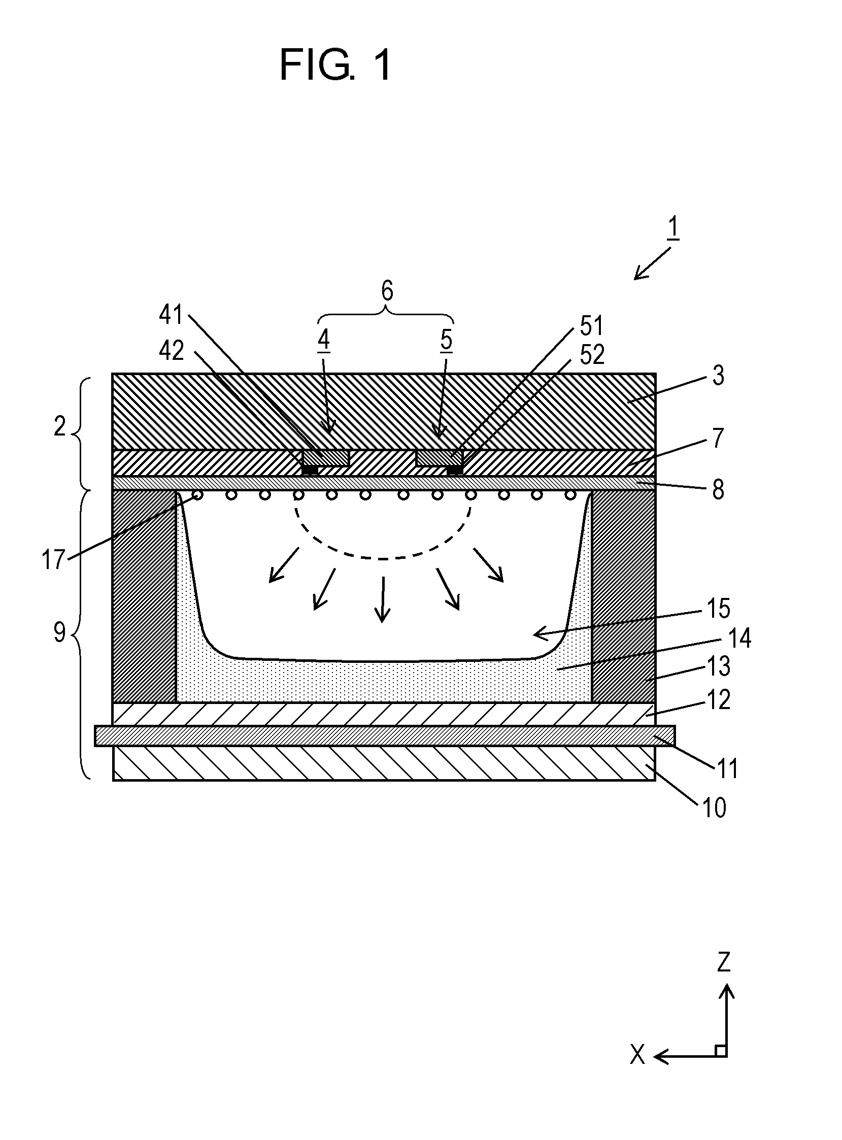
[0049]FIG. 1 is a schematic sectional view taken along the xz plane of PDP 1 of a first embodiment of the present invention. PDP 1 has a structure that is same as a conventional structure (FIG. 15) in general except for a structure of the periphery of protective film 8.

[0050]Here, PDP 1 is an AC type of the 42 inch class NTCS specification example, but the present invention may be applied to other specification examples such as XGA and SXGA as a matter of course. As a high definition PDP having a resolution higher than HD (High Definition), for example, the following specification can be shown. When the panel size is 37 inches, 42 inches, and 50 inches, the setting can be made to 1024×720 (pixel number), 1024×768 (pixel number) and 1366×768 (pixel number), respectively. In addition, a panel having a resolution higher than that of the HD panel can be included. As the panel having a resolution higher than HD, a full HD panel having 1920×1080 (pixel number) ca...

second embodiment

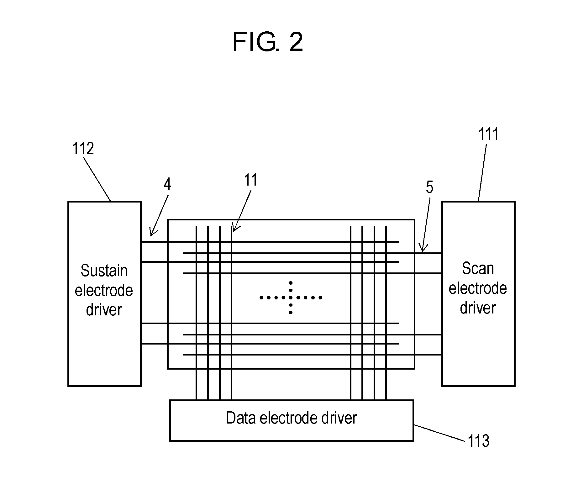
[0095]A second embodiment of the present invention will be described mainly about differences as compared to the first embodiment. FIG. 8 is a partially enlarged view (block diagram of the vicinity of a front panel at the time of driving) showing a structure of PDP 1a according to the second embodiment.

[0096]The basic structure of PDP 1a is similar to that of PDP 1, but is characteristic in that MgO fine particles 16 having high initial electron emission property are dispersed and arranged together with high γ fine particles 17 on the surface of protective film 8 facing discharge space 15. The dispersed densities of high γ fine particles 17 and MgO fine particles 16 can be set such that protective film 8 is not directly seen when the protective film in discharge cell 20 is two-dimensionally viewed from the Z direction, but are not limited thereto. For example, the particles may be partially provided, or may be provided only at positions corresponding to display electrode pairs 6.

[00...


PUM


Abstract

There is provided a PDP in which the structure of the periphery of a protective film is improved, excellent secondary electron emission property is exhibited, and improved efficiency and increased life can be expected. There is further provided a PDP in which occurrence of a discharge delay at the time of driving is prevented, and exhibition of high quality image display performance can be expected even in a high definition PDP that is driven at a high speed. Specifically, a crystalline film containing Sr in CeO2 in a concentration of 11.8 mol % to 49.4 mol % inclusive is formed on the surface of dielectric layer on the discharge space side as surface layer (protective film) having a thickness of about 1 μm. High γ fine particles having secondary electron emission property higher than those of protective film are arranged thereon.

Description

TECHNICAL FIELD[0001]The present invention relates to a plasma display panel using radiation by gas discharge, and particularly to a technique for improving properties of the periphery of a surface layer (protective film).BACKGROUND ART[0002]A plasma display panel (hereinafter referred to as a “PDP”) is a flat display device using radiation from gas discharge. Because of easy provision of high-speed display and upsizing, the PDP has been widely put into practical use in the fields of image display devices and public information display devices. The PDP is classified into a direct current type (DC type) and an alternating current type (AC type), but the surface-discharge type AC type PDP has an especially technical potential in terms of the life property and upsizing, and is commercialized.[0003]FIG. 15 is a schematic assembly diagram showing a structure of general AC type PDP 1x. PDR 1x shown in FIG. 15 is configured by laminating front panel 2 and back panel 9. Front panel 2 as a f...

Claims


Application Information

Patent Timeline
IPC IPC(8): H01J17/49H01J11/12H01J11/40
CPCH01J11/40H01J11/12
Inventor FUKUI, YUSUKENISHITANI, MIKIHIKOSAKAI, MASAHIROOKAFUJI, MICHIKOOKUI, YAYOIHONDA, YOSUKEYAMAUCHI, YASUHIROINOUE, OSAMUASANO, HIROSHI
Owner PANASONIC CORP
Why Eureka
Try Eureka