Hybrid photonic plasmonic interconnects (HyPPI) with intrinsic and extrinsic modulation options

a technology of photonic plasmonic interconnects and modulation options, which is applied in the field of photonic silicon-based waveguides, can solve the problems of easy melting of chips, no longer staying the physical properties of semiconductor materials, and severe limitations of on-chip communication interconnects, and achieves the effects of high operating frequency, reduced footprint, and improved interconnection performan

Active Publication Date: 2019-04-09
GEORGE WASHINGTON UNIVERSITY
View PDF0 Cites 0 Cited by
  • Summary
  • Abstract
  • Description
  • Claims
  • Application Information

AI Technical Summary

Benefits of technology

[0010]In light of these and other challenges, the present invention provides a Hybrid Photonic Plasmonic Interconnects (hereinafter referred to as “HyPPI”) strategy to combine photonics with plasmonic interconnect technology and show that this combination leads to superior link performance. In particular, the HyPPI includes four major parts, which are 1) nano-cavity plasmon lasers / LEDs with high operating frequencies and smaller footprints comparing with other regular lasers; 2) hybrid plasmon polaritons (HPPs) based electro-optic modulator (EOM) with relatively low insertion loss and impedance mismatch; 3) plasmonic photodetector with small footprint and relatively high responsivity and response speed; 4) silicon-based photonic waveguide with propagation loss less than 1 dB / cm, while its dimension based on the bit flow density (BFD) for specific applications.
[0011]The HyPPI technology is to hybridize the diffraction-limited photonic backbones with high LMI plasmonic active devices. However, hybrid plasmon polaritons have been used to overcome the high loss of traditional surface plasmon polaritons (SPPs) by using a silicon substrate under the active materials (i.e. indium-tin-oxide) to support part of the mode in the photonic waveguide and therefore decrease the coupling mismatch dramatically. Therefore, a single TE / TM mode light generated from the light source will propagate through the photonic waveguide, being coupled and modulated by the HPP EOM and couples back to the waveguide and finally being detected by the photodiode.
[0013]In addition, the high operating speed light source eliminates the need for an electro-optic modulator (EOM) if it is powerful enough to drive the entire link with high operating frequency under certain circumstances. This direct light source modulation is referred to as being “intrinsic” (vs. “extrinsic” for the EOM use), which allows source power management. Hybridization of classical photonic and nanophotonic elements is energy efficient (˜20 fJ / bit), low latency (<10 ps for millimeter-range propagation distances), reasonably long-range transmission (˜3 dB loss per length>104 μm) interconnect and a bit flow density up to 0.5 Gbps / μm2.

Problems solved by technology

The requirement of electronic device down-scaling has led to severe limitations for on-chip communication interconnects [1-3].
These effects are due to the heat generation in current integrated circuits, which can easily melt the chip.
Furthermore, the physical properties of semiconductor material will no longer stay the same once we reach 5 nm feature size.
Active optoelectronic devices based on pure photonic elements, however, often rely on optical non-linear physical effects requiring some form of light-matter-interaction (LMI), which is inherently weak, which often leads to significant power consumption.
Moreover, the sensitive ring-modulator based on high quality factor (Q factor) microrings is photon lifetime limited and bandwidth limited and requires heating to be tuned, which results in challenging dense integration.
Nonetheless, plasmonic interconnects are only suitable for short-distance communication purposes since its maximum propagation length is limited to tens of micrometers due to the ohmic loss of the plasmonic coherent electron oscillations at telecommunication frequencies.

Method used


Image

  • Hybrid photonic plasmonic interconnects (HyPPI) with intrinsic and extrinsic modulation options
  • Hybrid photonic plasmonic interconnects (HyPPI) with intrinsic and extrinsic modulation options
  • Hybrid photonic plasmonic interconnects (HyPPI) with intrinsic and extrinsic modulation options

Examples


Embodiment Construction

[0024]In describing a preferred embodiment of the invention illustrated in the drawings, specific terminology will be resorted to for the sake of clarity. However, the invention is not intended to be limited to the specific terms so selected, and it is to be understood that each specific term includes all technical equivalents that operate in similar manner to accomplish a similar purpose. Several preferred embodiments of the invention are described for illustrative purposes, it being understood that the invention may be embodied in other forms not specifically shown in the drawings.

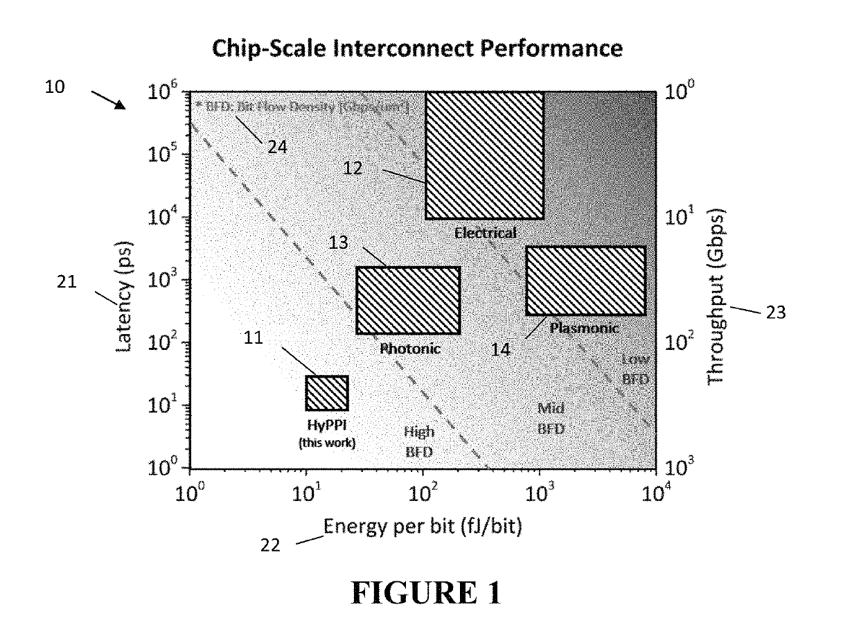
[0025]FIG. 1 is a representation of the improvement to latency 21, energy efficiency 22, throughput 23 and bit flow density 24 for the present invention. As shown, the HyPPI solution of the current invention 11 provides reduced latency and reduced energy consumption over traditional electrical 12, plasmonic 14 and photonic 13 solutions, while at the same time providing increased throughput and bit flow d...


PUM


Abstract

The Hybrid Photonic Plasmonic Interconnect (HyPPI) combines both low loss photonic signal propagation and passive routing with ultra-compact plasmonic devices. These optical interconnects therefore uniquely combine fast operational data-bandwidths (in hundreds of Gbps) for light manipulation with low optical attenuation losses by hybridizing low loss photonics with strong light-matter-interaction plasmonics to create, modulate, switch and detect light efficiently at the same time. Initial implementations were considered for on-chip photonic integration, but also promising for free space or fiber-based systems. In general two technical options exist, which distinguished by the method the electric-optic conversion is executed: the extrinsic modulation method consists of an continuous wave source such as an LED or laser operating at steady power output, and signal encoding is done via an electro-optic modulator downstream of the source in the interconnect. In contrast, in the intrinsic method, the optical source is directly amplitude modulated.

Description

RELATED APPLICATIONS[0001]This application claims the benefit to U.S. Provisional Application No. 62 / 387,218, filed Dec. 24, 2015 and U.S. Provisional Application No. 62 / 387,143, filed Dec. 23, 2015, of which their entities are incorporated herein by reference.GOVERNMENT LICENSE RIGHTS[0002]This invention was made with Government support under Grant / Contract No. FA9550-15-1-0447 awarded by Air Force Office of Scientific Research (AFOSR). The U.S. Government has certain rights in this invention.BACKGROUND OF THE INVENTIONField of the Invention[0003]The present invention relates to a photonic silicon-based waveguide with plasmonic-integrated devices hybridization for high speed, energy efficiency and small footprint on-chip interconnects in the field of optical communication and data processing. Moreover, such interconnect is able to be applied for both intra-chip and inter-chip interconnects.Background of the Related Art[0004]The requirement of electronic device down-scaling has led ...

Claims


Application Information

Patent Timeline
Patent Type & Authority Patents(United States)
IPC IPC(8): H01S5/00H01S5/10H01S5/042G02B6/12
CPCH01S5/0014G02B6/12004H01S5/1046H01S5/0427G02B2006/12123G02B2006/12121G02B6/1226H04B10/801
Inventor SUN, SHUAISORGER, VOLKER J.EL-GHAZAWI, TAREKNARAYANA, VIKRAM K.BADAWY, ABDEL-HAMEED A.
Owner GEORGE WASHINGTON UNIVERSITY
Why Eureka
Try Eureka