Method of reducing plasma arcing on surfaces of semiconductor processing apparatus components in a plasma processing chamber

a technology of semiconductor processing apparatus and plasma processing chamber, which is applied in the field of yttrium oxidecomprising ceramic, can solve the problems of shortening the life span of protective coating, reducing electrical resistivity, and anodizing layer, and achieves tailoring mechanical properties and improved plasma resistance.

Inactive Publication Date: 2013-01-24
APPLIED MATERIALS INC
View PDF2 Cites 28 Cited by
  • Summary
  • Abstract
  • Description
  • Claims
  • Application Information

AI Technical Summary

Benefits of technology

[0011]Specialty sintered ceramic materials have been developed which resist corrosion under semiconductor processing conditions which employ a halogen-containing plasma. The specialty materials have been modified to have improved plasma resistance and tailored mechanical properties in comparison with the sintered ceramic materials previously used for semiconductor processing apparatus. The electrical properties of the sintered ceramic materials have been adjusted so that the electrical resistivity properties of the materials (which have an effect in a plasma processing chamber) meet the requirements of critical chamber components. These electrical resistivity property requirements were previously met only by materials which exhibited low plasma resistance properties. The present specialty materials (which offer various combinations of plasma resistance, mechanical properties, and electrical resistivity properties) are sufficiently similar to those of semiconductor processing apparatus previously used. One advantage of the similar electrical properties is that it is not necessary to change the process recipes or general processing conditions which are currently in use in semiconductor device fabrication.
[0014]One of the major components in a semiconductor processing chamber which requires a lower resistivity than is typical for yttrium-comprising sintered ceramics is the electrostatic chuck. The electrostatic chuck designers recommend that the resistivity of the dielectric surface of the electrostatic chuck fall within a range from about 109 to 1011 Ω·cm under semiconductor processing conditions, to reduce the possibility of plasma arcing at the electrostatic chuck. This resistivity range is equivalent to a conductivity within a range from about 10−9 to 10−7 S / m. This is a considerably lower resistivity than bulk Si3N4, for example, which exhibits a conductivity of 10−13 S / m. For other corrosion resistant surfaces where plasma arcing might be a problem, such as lift pins, a resistivity in the range of that required for an electrostatic chuck is helpful. For corrosion resistant surfaces such as process chamber liners, the resistivity may be higher, possibly as high as or exceeding about 1014 Ω·cm and still be acceptable.

Problems solved by technology

However, the integrity of the anodization layer may be deteriorated by impurities in the aluminum or aluminum alloy, so that corrosion begins to occur early, shortening the life span of the protective coating.
The positive ions of the other oxides have a different valence from the Y3+ ion, to form a Y vacancy, leading to a decrease of electrical resistivity.
This results in an O vacancy, which also decreases electrical resistivity.

Method used


Image

  • Method of reducing plasma arcing on surfaces of semiconductor processing apparatus components in a plasma processing chamber
  • Method of reducing plasma arcing on surfaces of semiconductor processing apparatus components in a plasma processing chamber
  • Method of reducing plasma arcing on surfaces of semiconductor processing apparatus components in a plasma processing chamber

Examples


examples

[0038]

TABLEPrecursorWeightMeltingSinteringPrecursorPrecursorParts / 100PointTemp.PhaseDensitySample #Molar %Weight %Y2O3(° C.)(° C.)Comp.(g / cm3)1Y2O3: 75.0Y2O3: 77.82Y2O3: 100.002800>1800c-ss5.607HfO2: 20.0HfO2: 19.35HfO2: 24.86singleZrO2: 5.0ZrO2: 2.83ZrO2: 3.64phase**2Y2O3: 60.0Y2O3: 72.18Y2O3: 100.002360>1800c-ss4.936Sc2O3: 20.0Sc2O3: 14.69Sc2O3: 20.36singleZrO2: 20.0ZrO2: 13.13ZrO2: 18.19phase**3Y2O3: 60.0Y2O3: 59.58Y2O3: 100.00N / A*>1800c-ss5.555Nd2O3: 20.0Nd2O3: 29.58Nd2O3: 49.66singleZrO2: 20.0ZrO2: 10.84ZrO2: 18.19phase**4Y2O3: 70.0Y2O3: 75.53Y2O3: 100.00N / A*>1800c-ss**5.331Nb2O5: 10.0Nb2O5: 12.7Nb2O5: 16.82Y3NbOZrO2: 20.0ZrO2: 11.77ZrO2: 15.59and Nb*N / A = not available**c-ss means cubic yttria type solid solution.

example one

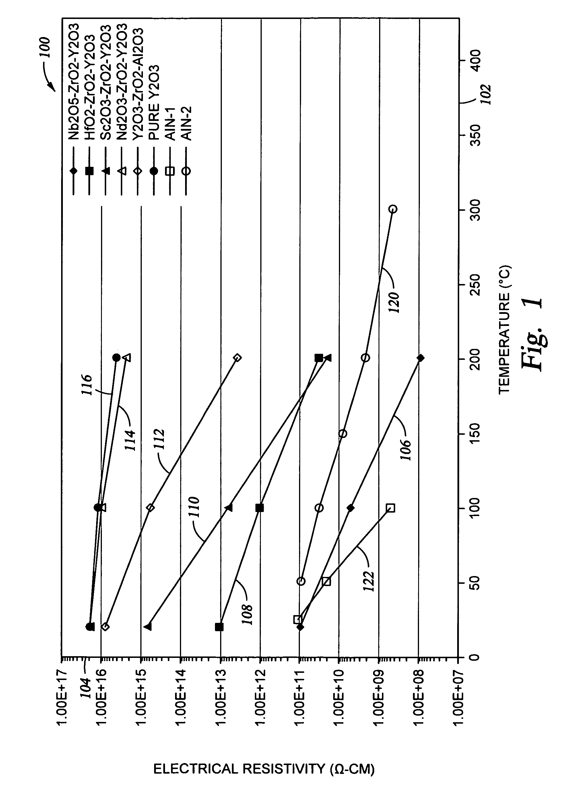
[0039]FIG. 1 shows a graph 100 illustrating electrical resistivity of a variety of ceramic materials, including the Type A and Type B materials made according to exemplary embodiments of the invention. The resistivity is shown on axis 104, as a function of temperature, which is shown on axis 102. The resistivity was measured at 1000 V in an air environment, using standard test conditions in accordance with ASTM D 1829-66 or JIS C2141.

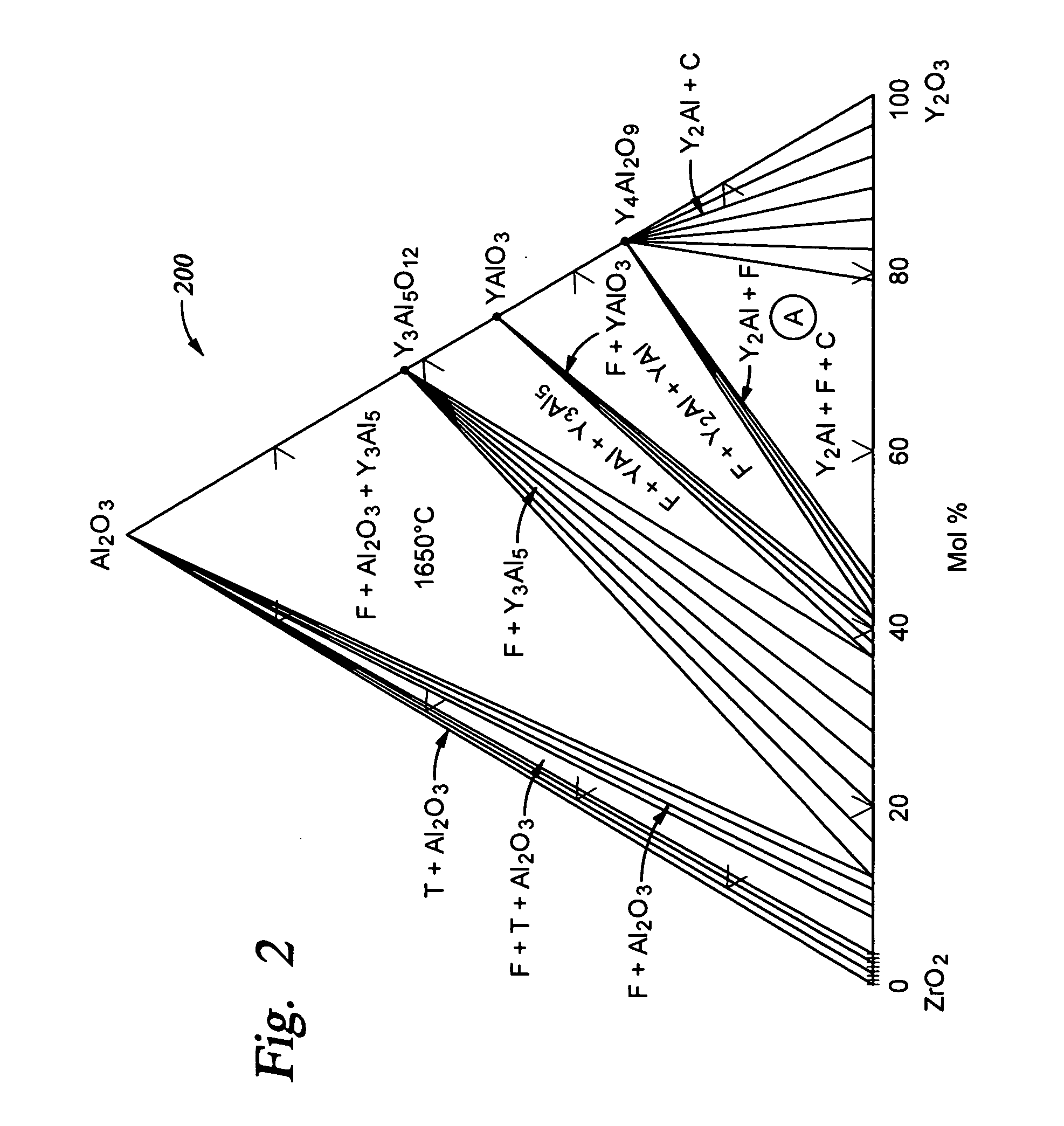
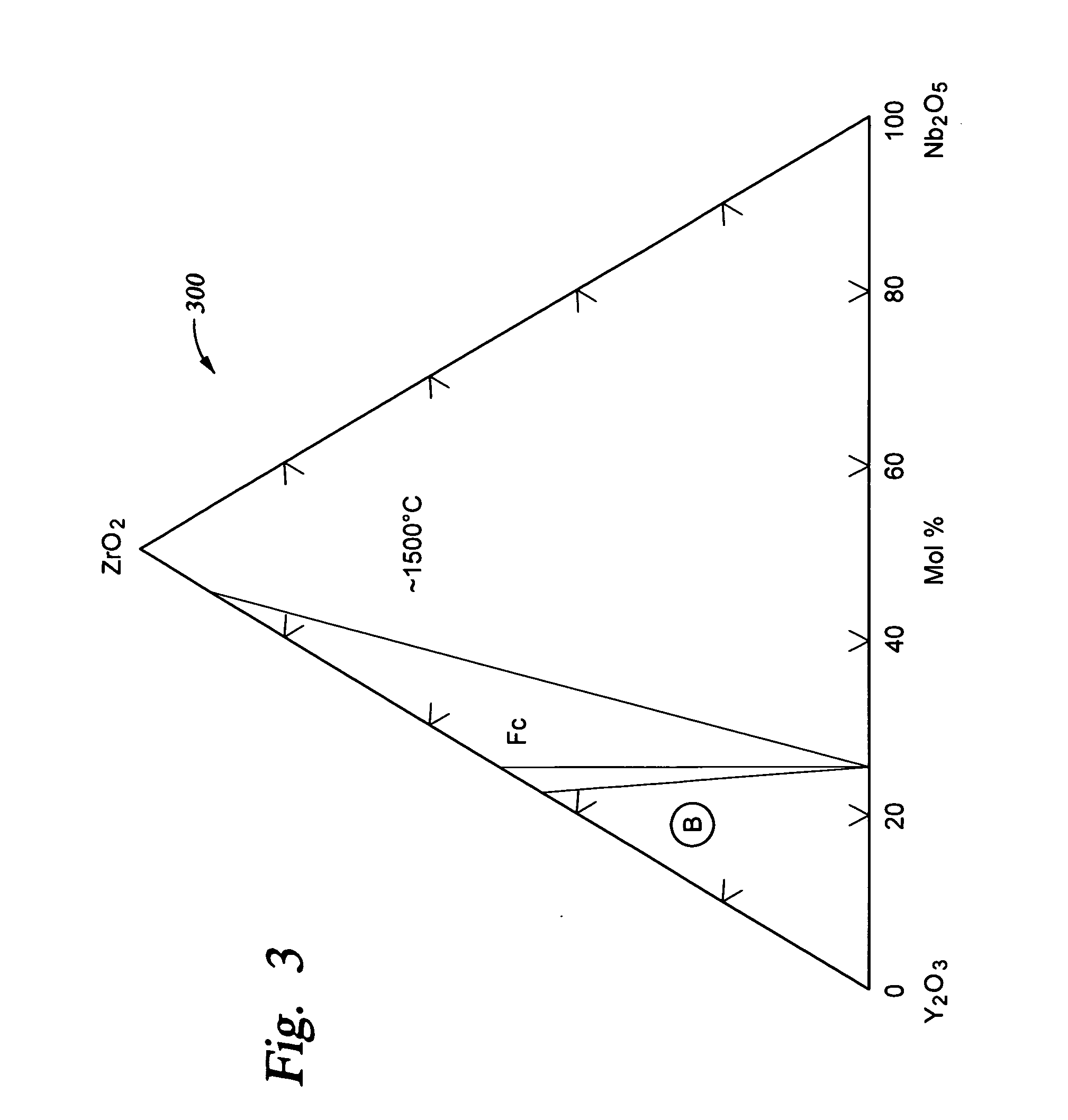
[0040]Curve 106 shown in FIG. 1 is representative of the Nb2O5-comprising sintered ceramic material which is described as Sample #4 in the Table. With respect to sintered ceramic material comprising Nb2O5, acceptable electrical resistivity values are expected to be obtained for additional compositions as well, as illustrated by the phase diagram shown in FIG. 3. The sintered ceramic material contains three phases, which include a first phase solid solution comprising Y2O3—ZrO2—Nb2O5 which may make up about 60 molar % to about 90 molar % of the sintered ...

example two

[0042]Curve 108 shown in FIG. 1 is representative of the HfO2 -comprising sintered ceramic material, made in accordance with the present invention, which is also described as Sample #1 in the Table. This ceramic material exhibits a higher resistivity than the Nb2O5-comprising material, but is useful for fabricating semiconductor processing apparatus components where arcing is less critical than with respect to an electrostatic chuck or a substrate lift pin.


PUM

PropertyMeasurementUnit
temperatureaaaaaaaaaa
electrical resistivityaaaaaaaaaa
thicknessaaaaaaaaaa

Abstract

Specialty ceramic materials which resist corrosion / erosion under semiconductor processing conditions which employ a corrosive / erosive plasma. The corrosive plasma may be a halogen-containing plasma. The specialty ceramic materials have been modified to provide a controlled electrical resistivity which suppresses plasma arcing potential.

Description

[0001]This application is a divisional application of U.S. application Ser. No. 11 / 890,156, filed Aug. 2, 2007, and entitled: “Plasma-Resistant Ceramics With Controlled Electrical Resistivity”, which is currently pending.[0002]The present application is related to a series of applications which have common inventorship with the present application. All of the applications listed below relate to the use of a yttrium-oxide comprising ceramic to provide a plasma-resistant surface which is useful in semiconductor processing apparatus. The related applications include U.S. application Ser. No. 11 / 796,210, of Sun et al., filed Apr. 27, 2007, titled: “Method of Reducing The Erosion Rate Of Semiconductor Processing Apparatus Exposed To Halogen-Containing Plasmas”, which is now abandoned; U.S. application Ser. No. 11 / 796,211, of Sun et al., filed Apr. 27, 2007, titled: “Method And Apparatus Which Reduce The Erosion Rate Of Surfaces Exposed To Halogen-Containing Plasmas”, which issued as U.S....

Claims


Application Information

Patent Timeline
Patent Type & Authority Applications(United States)
IPC IPC(8): C04B35/505B32B18/00
CPCC04B35/486Y10T428/31C04B35/50C04B35/505C04B2235/3217C04B2235/3222C04B2235/3224C04B2235/3225C04B2235/3229C04B2235/3244C04B2235/3251C04B2235/3255C04B2235/404C04B2235/762C04B2235/77C04B2235/80C04B2235/81C04B35/495H01L21/205
Inventor SUN, JENNIFER Y.COLLINS, KENNETH S.DUAN, REN-GUANTHACH, SENHGRAVES, THOMASHE, XIAOMINGYUAN, JIE
Owner APPLIED MATERIALS INC
Why Eureka
Try Eureka