Semiconductor integrated circuit device

a technology of integrated circuits and semiconductors, applied in the direction of instruments, computations using denominational number representations, pulse techniques, etc., can solve the problem of large chip area, and achieve the effect of suppressing leakage current and increasing chip area

Inactive Publication Date: 2013-01-31
SOCIONEXT INC
View PDF9 Cites 20 Cited by
  • Summary
  • Abstract
  • Description
  • Claims
  • Application Information

AI Technical Summary

Benefits of technology

[0011]An object of the present invention is therefore to provide a semiconductor integrated circuit device that can efficiently suppress leak current without increasing a chip area.
[0013]According to this aspect, the semiconductor integrated circuit device includes the first, second, and third standard cells that have the same logic. The second standard cell has a cell width larger than that of the first standard cell, but a gate length of a MOS transistor constituting a circuit is equal to that of the first standard cell. The third standard cell has a cell width equal to that of the second standard cell, but a shape of a gate of a MOS transistor constituting a circuit is different from that of the second standard cell. That is, the third standard cell has a MOS transistor having a gate length longer than that of the first and second standard cells. Accordingly, leak current becomes small although a circuit delay becomes large, as compared with first and second standard cells. Therefore, by replacing the first standard cell adjacent to a space area with the second standard cell, and by replacing the second standard cell in a path having room in timing with the third standard cell, for example, leak current can be suppressed without increasing a chip area.
[0017]According to this aspect, the semiconductor integrated circuit device includes the first and second standard cells that have the same logic. The first standard cell has a first parallel transistor group including two or more MOS transistors connected in parallel, and having gates connected in common. The second standard cell has the same cell width as that of the first standard cell, and has a second parallel transistor group corresponding to the first parallel transistor group. The second parallel transistor group includes two or more MOS transistors connected in parallel, and having gates connected in common, and has at least one MOS transistor having the parallel number smaller than that of the first parallel transistor group and having a gate length larger than that of the first parallel transistor group. Accordingly, in the second standard cell, leak current becomes small although a circuit delay becomes large, as compared with the first standard cell. Therefore, for example, by replacing the first standard cell in a path having room in timing with the second standard cell, leak current can be efficiently suppressed without increasing a chip area.
[0020]According to the present invention, a semiconductor integrated circuit device has layout generated by combining plural standard cells in which layout such as a cell width and a gate length is properly adjusted. Therefore, leak current can be suppressed without increasing a chip area, and without turning back in a design.

Problems solved by technology

When a standard cell like this is used, there occurs a problem that a chip area becomes large as a result.

Method used


Image

  • Semiconductor integrated circuit device
  • Semiconductor integrated circuit device
  • Semiconductor integrated circuit device

Examples


first exemplary embodiment

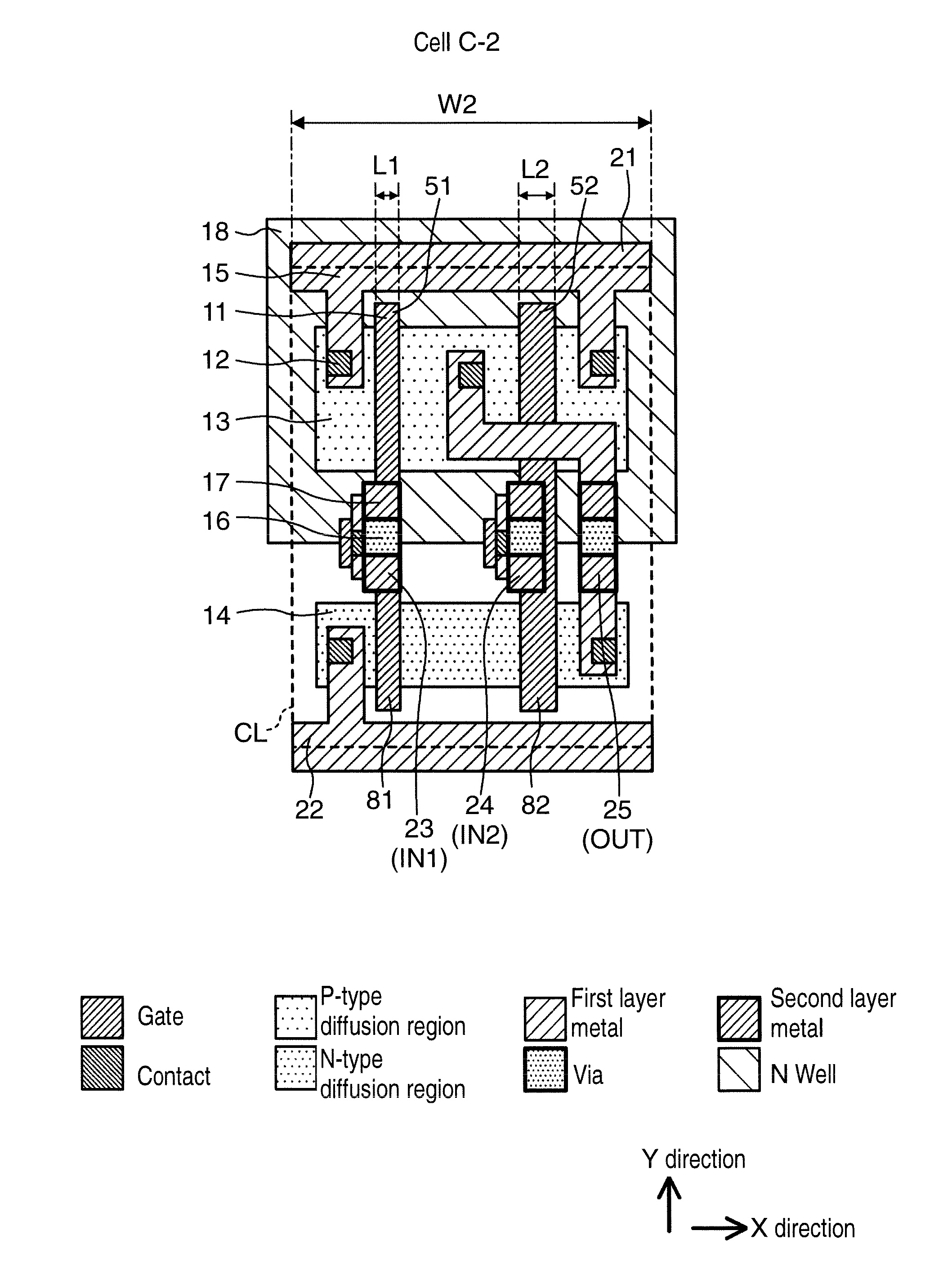
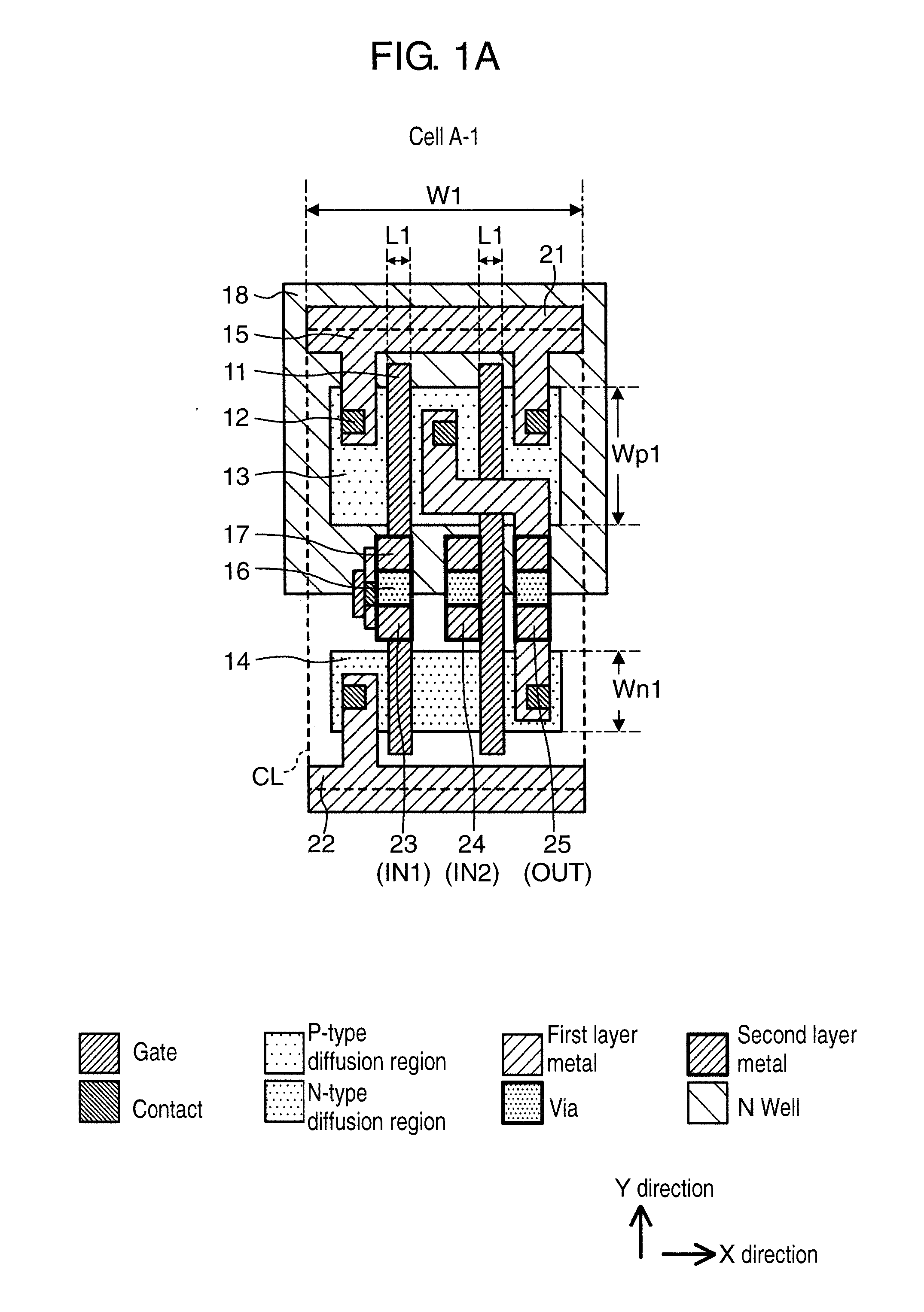
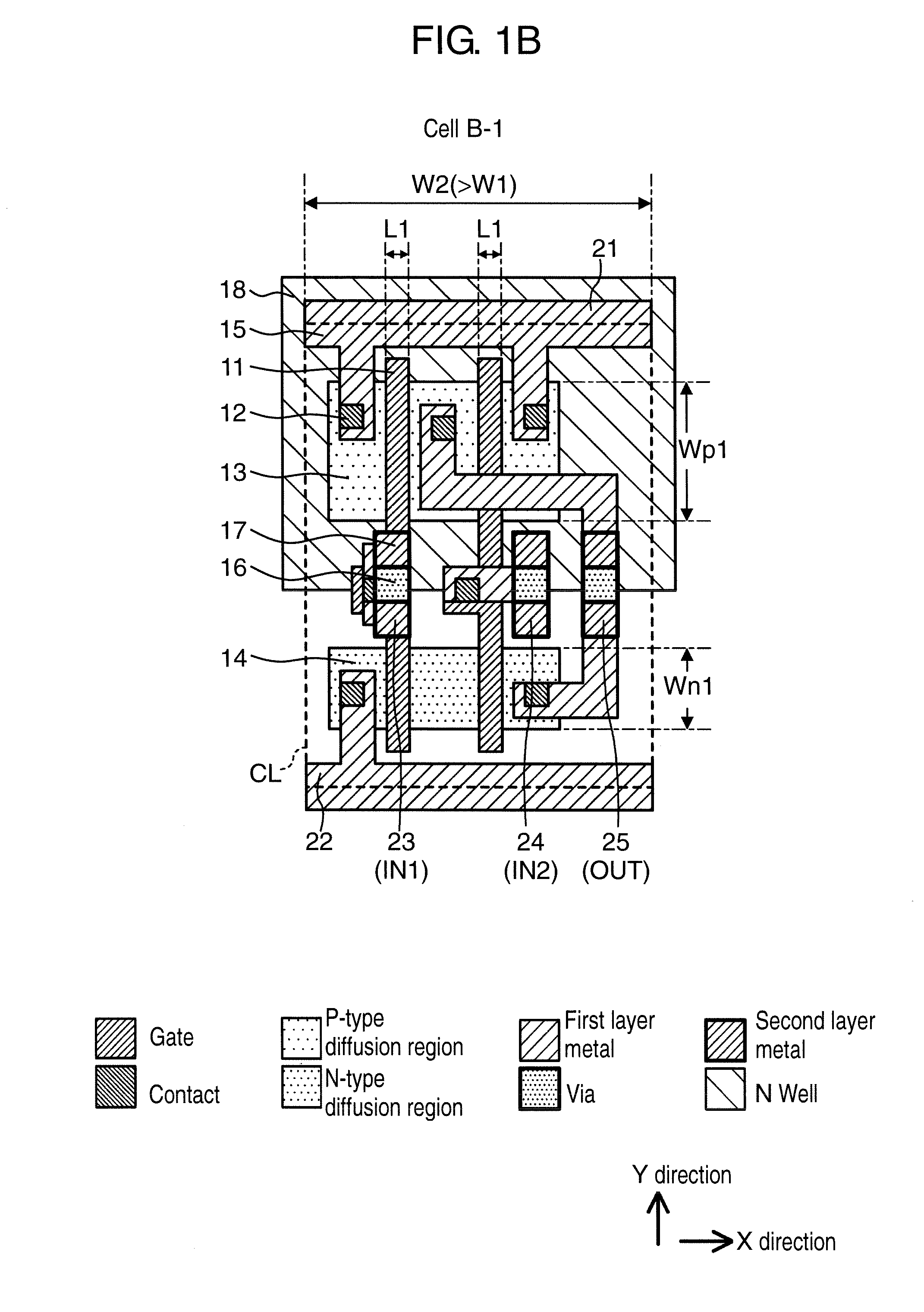
[0044]FIGS. 1A, 1B, and 1C are plan views showing layout examples of a standard cell to be used in a semiconductor integrated circuit device according to a first exemplary embodiment. Cell A-1 in FIG. 1A, cell B-1 in FIG. 1B, and cell C-1 in FIG. 1C are all standard cells of the same logic, and show examples of a two-input NAND cell in this case.

[0045]In FIGS. 1A, 1B, and 1C, 11 denotes a gate of a MOS transistor, 12 denotes a contact, 13 denotes a P-type diffusion region, 14 denotes an N-type diffusion region, 15 denotes a first layer metal, 16 denotes a via that connects between the first layer metal and a second layer metal, 17 denotes the second layer metal, and 18 denotes an N-well region. Contact 12 connects between the gate or a diffusion layer and the first layer metal. As circuit elements, 21 denotes a power source line to which a power source potential is supplied, 22 denotes a ground line, 23 denotes a terminal wiring that becomes an input terminal (IN1), 24 denotes a ter...

second exemplary embodiment

[0065]FIGS. 6A and 6B are plan views showing layout examples of a standard cell to be used in a semiconductor integrated circuit device according to a second exemplary embodiment. Cell B-2 in FIG. 6A and cell C-3 in FIG. 6B are standard cells of the same logic as that of cell A-1 and the like shown in FIGS. 1A to 1C, and are two-input NAND cells. In FIGS. 6A and 6B, constituent elements that are common to those in FIGS. 1A to 1C are attached with the same reference symbols as those in FIG. 1, and their detailed description is omitted here.

[0066]Cell B-2 in FIG. 6A is designed such that a gate length and a gate width are equal to those of cell A-1 in FIG. 1A and that a delay time of the circuit is the same as that of cell A-1. However, a main difference is that cell B-2 has a cell width larger than that of cell A-1. That is, cell B-2 has cell width W3 larger than W1 (W3>W1), a gate length of a MOS transistor that constitutes a circuit is L1 which is the same as the gate length of cel...

third exemplary embodiment

[0073]FIGS. 8A and 8B are plan views showing layout examples of a standard cell to be used in a semiconductor integrated circuit device according to a third exemplary embodiment. Cell A-2 in FIG. 8A and cell D-1 in FIG. 8B are standard cells of the same logic, and show examples of an inverter cell in this case.

[0074]In FIGS. 8A and 8B, 11 denotes a gate of a MOS transistor, 12 denotes a contact, 13 denotes a P-type diffusion region, 14 denotes an N-type diffusion region, 15 denotes a first layer metal, 16 denotes a via that connects between the first layer metal and a second layer metal, 17 denotes the second layer metal, and 18 denotes an N-well region. Contact 12 connects between the gate or a diffusion layer and the first layer metal. As circuit elements, 21 denotes a power source line to which a power source potential is supplied, 22 denotes a ground line, 26 denotes a terminal wiring that becomes an input terminal (IN), 27 denotes a terminal wiring that becomes an output termin...


PUM


Abstract

A semiconductor integrated circuit device includes cells A-1, B-1, and C-1 that have the same logic. Cell B-1 has cell width W2 larger than a cell width of cell A-1, but gate length L1 of a MOS transistor is equal to that of cell A-1. Cell C-1 has cell width W2 equal to a cell width of cell B-1, but has a MOS transistor having large gate length L2. A circuit delay of cell C-1 becomes large as compared with that of cells A-1 and B-1, but leak current becomes small. Therefore, by replacing cell A-1 adjacent to a space area with cell B-1, and by replacing cell B-1 in a path having room in timing with cell C-1, for example, leak current can be suppressed without increasing a chip area.

Description

BACKGROUND[0001]1. Field of the Invention[0002]The present invention relates to a semiconductor integrated circuit device, and particularly relates to a semiconductor integrated circuit device that is formed by a layout design using a standard cell system.[0003]2. Description of the Related Art[0004]In a layout design of a semiconductor integrated circuit device using a standard cell system, a layout generation tool called a place and route tool (P and R tool) is used. The automatic layout wiring tool is for obtaining a desired semiconductor integrated circuit device, by registering in advance standard cells into a standard cell library as a database, reading data of the standard cells of a desired basic circuit from the database, and arraying and wiring the data in a predetermined region. In the standard cells, there are cells such as an inverter, a NAND, and an NOR that achieve mutually different logics and functions. For a majority of the standard cells that are included in the s...

Claims


Application Information

Patent Timeline
Patent Type & Authority Applications(United States)
IPC IPC(8): H01L25/00
CPCH01L27/0207H01L2027/11822H01L27/11807
Inventor ANDO, TAKASHIKUSUMOTO, KEIICHISHIMAZAKI, KENJINAKANISHI, KAZUYUKITOUBOU, TETSUROU
Owner SOCIONEXT INC
Why Eureka
Try Eureka