
Semiconductor integrated circuit device having a plurality of standard cells for leakage current suppression
a technology of integrated circuit and standard cells, which is applied in the direction of instruments, computations using denominational number representation, pulse techniques, etc., can solve the problem of large chip area, and achieve the effect of suppressing leakage current and increasing chip area
- Summary
- Abstract
- Description
- Claims
- Application Information
AI Technical Summary
Benefits of technology
Problems solved by technology
Method used
Image

Examples
first exemplary embodiment
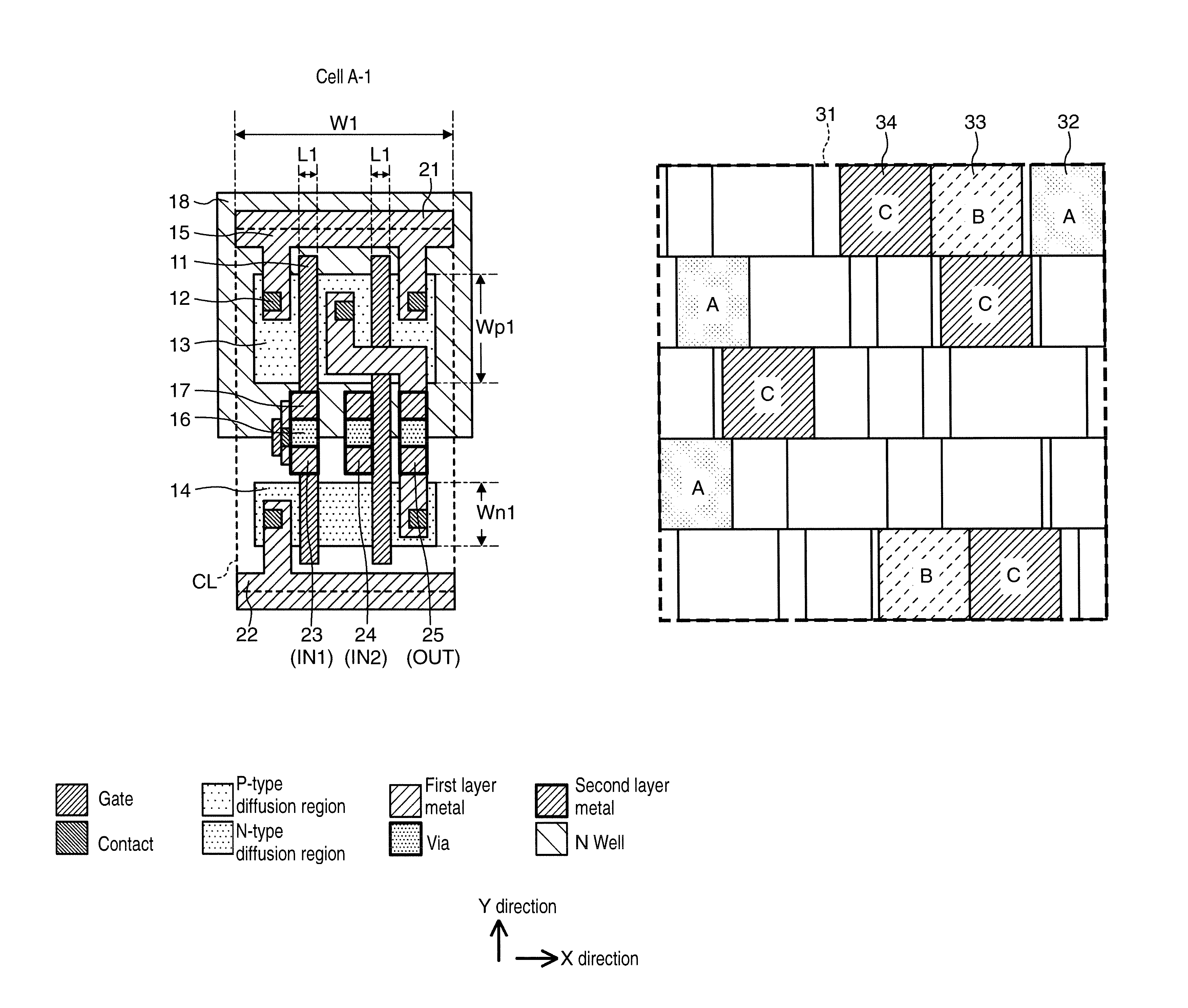
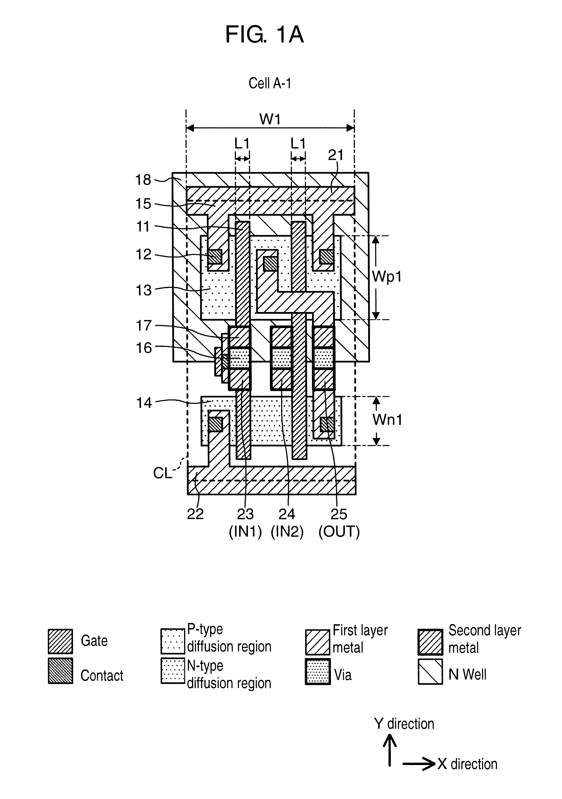
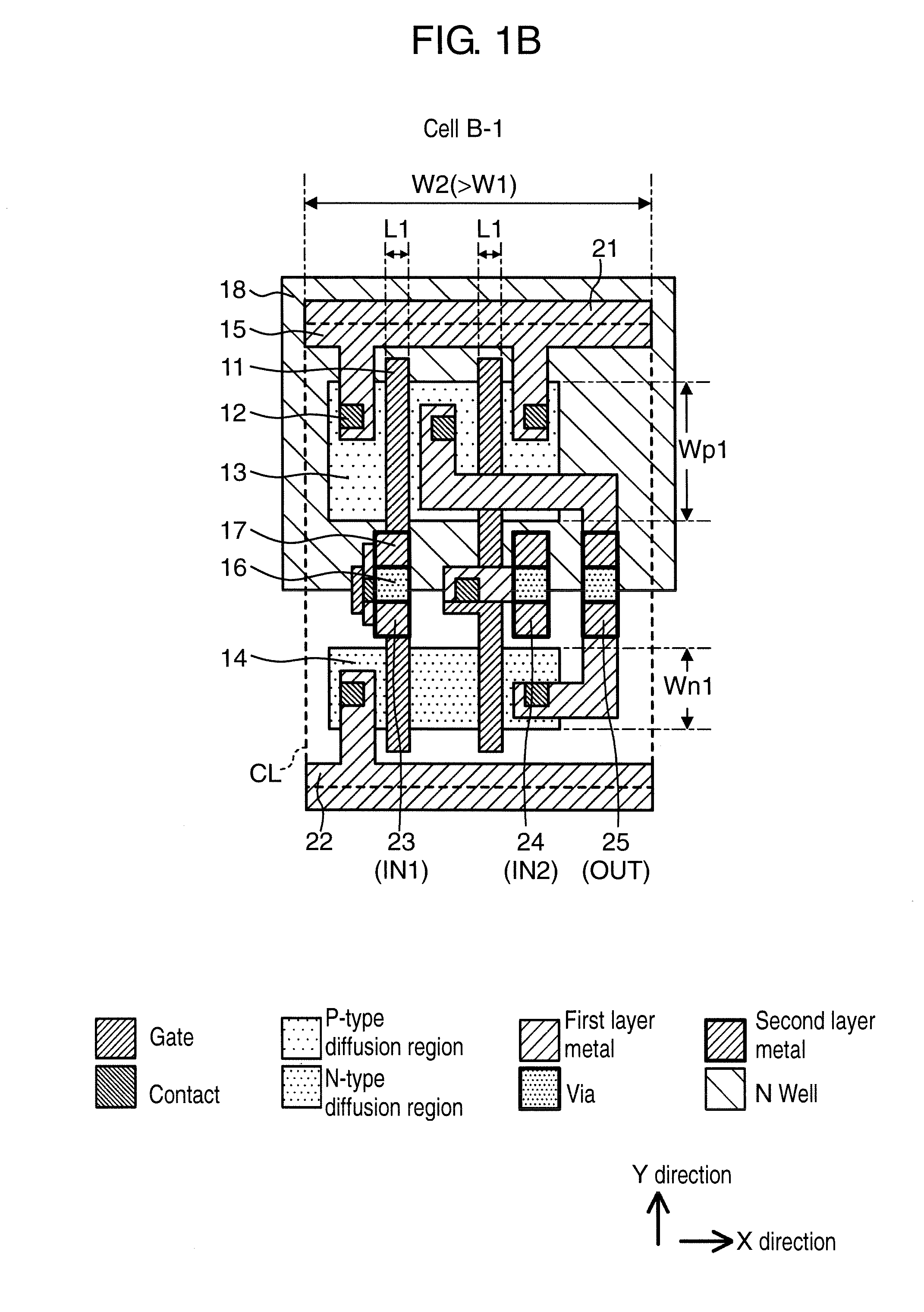
[0044]FIGS. 1A, 1B, and 1C are plan views showing layout examples of a standard cell to be used in a semiconductor integrated circuit device according to a first exemplary embodiment. Cell A-1 in FIG. 1A, cell B-1 in FIG. 1B, and cell C-1 in FIG. 1C are all standard cells of the same logic, and show examples of a two-input NAND cell in this case.
[0045]In FIGS. 1A, 1B, and 1C, 11 denotes a gate of a MOS transistor, 12 denotes a contact, 13 denotes a P-type diffusion region, 14 denotes an N-type diffusion region, 15 denotes a first layer metal, 16 denotes a via that connects between the first layer metal and a second layer metal, 17 denotes the second layer metal, and 18 denotes an N-well region. Contact 12 connects between the gate or a diffusion layer and the first layer metal. As circuit elements, 21 denotes a power source line to which a power source potential is supplied, 22 denotes a ground line, 23 denotes a terminal wiring that becomes an input terminal (IN1), 24 denotes a ter...
second exemplary embodiment
[0065]FIGS. 6A and 6B are plan views showing layout examples of a standard cell to be used in a semiconductor integrated circuit device according to a second exemplary embodiment. Cell B-2 in FIG. 6A and cell C-3 inFIG. 6B are standard cells of the same logic as that of cell A-1 and the like shown in FIGS. 1A to 1C, and are two-input NAND cells. In FIGS. 6A and 6B, constituent elements that are common to those in FIGS. 1A to 1C are attached with the same reference symbols as those in FIG. 1, and their detailed description is omitted here.
[0066]Cell B-2 in FIG. 6A is designed such that a gate length and a gate width are equal to those of cell A-1 in FIG. 1A and that a delay time of the circuit is the same as that of cell A-1. However, a main difference is that cell B-2 has a cell width larger than that of cell A-1. That is, cell B-2 has cell width W3 larger than W1 (W3>W1), a gate length of a MOS transistor that constitutes a circuit is L1 which is the same as the gate length of cell...
third exemplary embodiment
[0073]FIGS. 8A and 8B are plan views showing layout examples of a standard cell to be used in a semiconductor integrated circuit device according to a third exemplary embodiment. Cell A-2 in FIG. 8A and cell D-1 in FIG. 8B are standard cells of the same logic, and show examples of an inverter cell in this case.
[0074]In FIGS. 8A and 8B, 11 denotes a gate of a MOS transistor, 12 denotes a contact, 13 denotes a P-type diffusion region, 14 denotes an N-type diffusion region, 15 denotes a first layer metal, 16 denotes a via that connects between the first layer metal and a second layer metal, 17 denotes the second layer metal, and 18 denotes an N-well region. Contact 12 connects between the gate or a diffusion layer and the first layer metal. As circuit elements, 21 denotes a power source line to which a power source potential is supplied, 22 denotes a ground line, 26 denotes a terminal wiring that becomes an input terminal (IN), 27 denotes a terminal wiring that becomes an output termin...
PUM
 Abstract
Description
Claims
Application Information