Electronic device and method for manufacturing same
- Summary
- Abstract
- Description
- Claims
- Application Information
AI Technical Summary
Benefits of technology
Problems solved by technology
Method used
Image

Examples
first embodiment
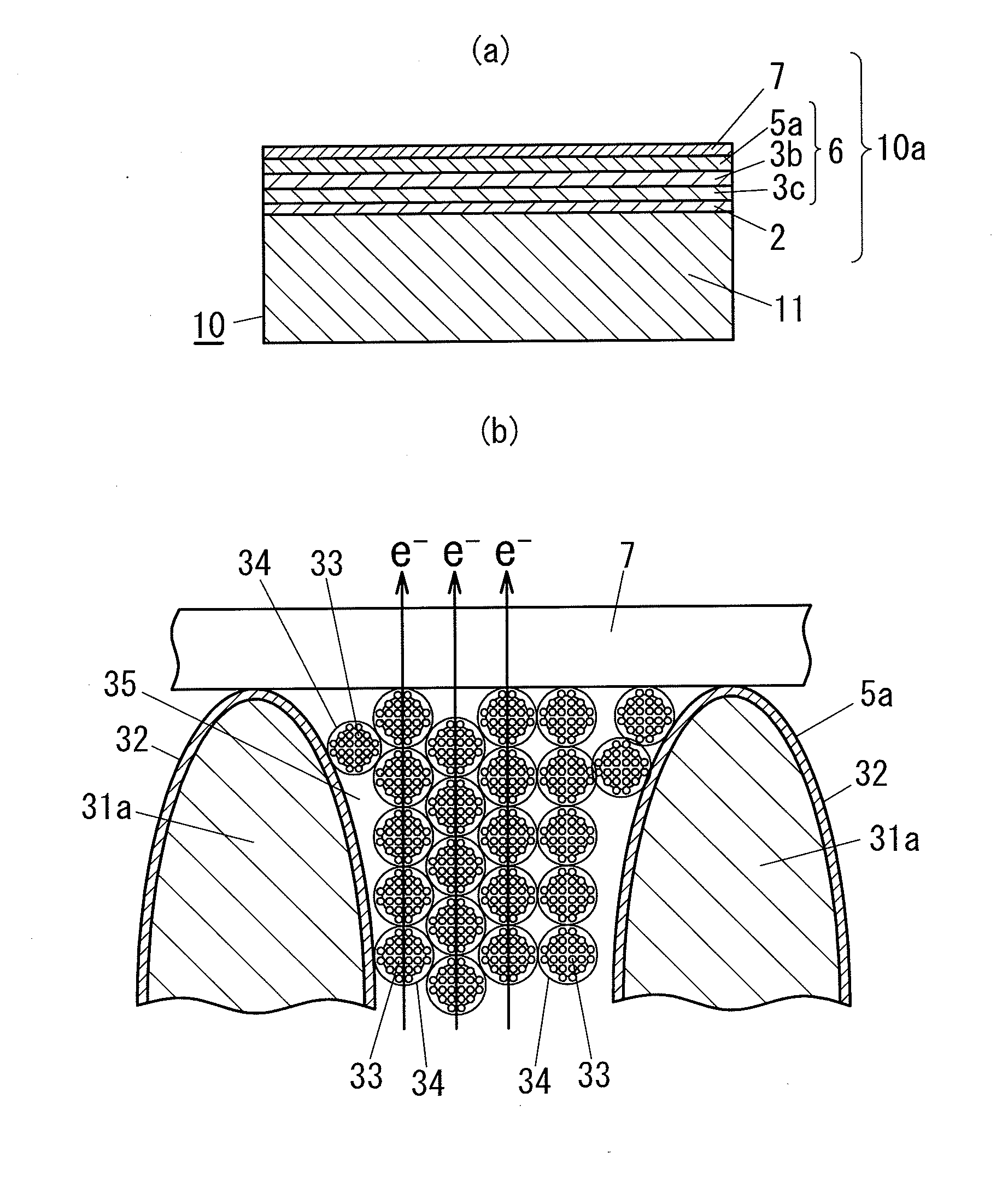
[0025]The following explanation referring FIG. 1 is made to the electronic device of the present embodiment.
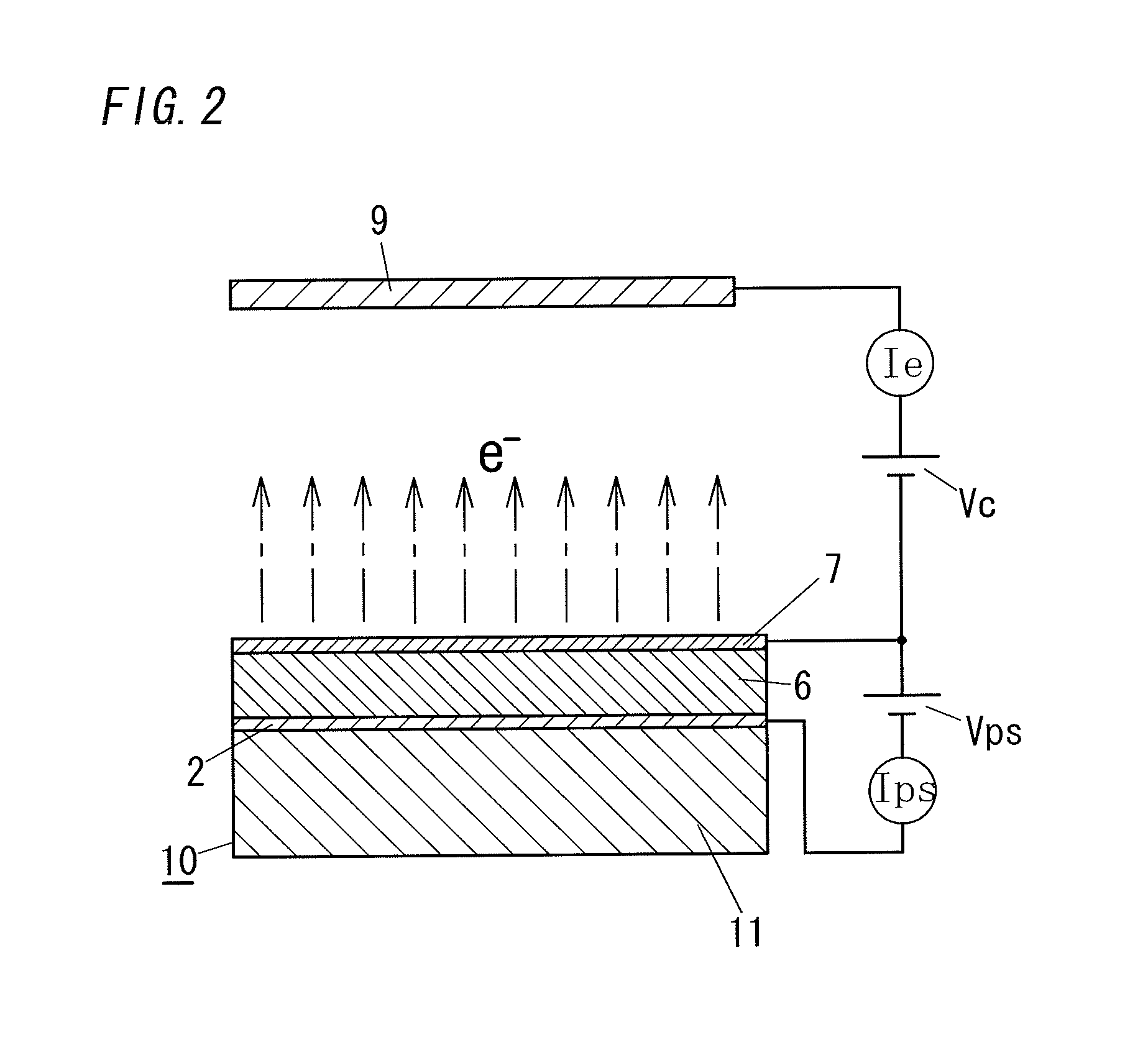
[0026]The electronic device includes a substrate 11, a lower electrode 2, a surface electrode 7, and a functional layer 5a. The lower electrode 2 is defined as a first electrode formed over a surface of the substrate 11. The surface electrode 7 is defined as a second electrode located on an opposite side of the lower electrode 2 from the substrate 11 so as to face the lower electrode 2. The functional layer 5a is interposed between the lower electrode 2 and the surface electrode 7, and is formed by means of anodizing a first polycrystalline semiconductor layer 3a (see FIG. 2 (c)) in an electrolysis solution so as to contain plural semiconductor nanocrystals 33. Further, the electronic device includes a second polycrystalline semiconductor layer 3b. The second polycrystalline semiconductor layer 3b is interposed between the lower electrode 2 and the functional layer 5a so as to...
second embodiment
[0054]The electronic device of the present embodiment has the same basic configuration as the first embodiment. The electronic device of the present embodiment is different from the first embodiment in that the third polycrystalline semiconductor layer 3c (see FIG. 1 (a)) as explained in the first embodiment is not provided and the second polycrystalline semiconductor layer 3b is directly formed on the lower electrode 2, for example. Besides, components common to the present embodiment and the first embodiment are designated by the same reference numerals, and explanations thereof are deemed unnecessary
[0055]The following explanation referring FIG. 5 is made to a method of manufacturing the electron source 10 defining the electronic device. However, explanations are not made to steps common to the manufacturing method of the present embodiment and the manufacturing method explained in the first embodiment.
[0056]First, the lower electrode 2 having the first predetermined thickness (e...
third embodiment
[0065]The present embodiment shows a light emitting device configured to emit light based on a quantum effect caused by electric field excitation, as an example of the electronic device.
[0066]The light emitting device 20 of the present embodiment as illustrated in FIG. 6 (a) has the approximately same basic configuration as the electron source 10 of the second embodiment. The light emitting device 20 of the present embodiment is different from the electron source 10 of the second embodiment in that the functional layer 5a interposed between the lower electrode 2 and the surface electrode 7 acts as a light emitting layer 16 and the surface electrode 7 is designed to transmit light emitted from the light emitting layer 16. Besides, components common to the present embodiment and the second embodiment are designated by the same reference numerals, and explanations thereof are deemed unnecessary
[0067]For example, the surface electrode 7 is constituted by a transparent conductive film. T...
PUM
 Abstract
Description
Claims
Application Information
 - R&D Engineer
- R&D Manager
- IP Professional
- Industry Leading Data Capabilities
- Powerful AI technology
- Patent DNA Extraction
Browse by: Latest US Patents, China's latest patents, Technical Efficacy Thesaurus, Application Domain, Technology Topic.
© 2024 PatSnap. All rights reserved.Legal|Privacy policy|Modern Slavery Act Transparency Statement|Sitemap