Component having a multipactor-inhibiting carbon nanofilm thereon, apparatus including the component, and methods of manufacturing and using the component

a carbon nanofilm, multi-pactor technology, applied in the manufacture of transit tubes/containers, electrode systems, electric discharge tubes/lamps, etc., can solve the problems of reducing overall performance, multi-pactor flashover events at relatively low field strengths, and avalanche of electrons that damage or destroy components of high-power rf energy devices, etc., to improve the reliability of components, reduce electromagnetic energy transmission, and improve the effect of reliability

Active Publication Date: 2013-02-07
NOKOMIS
View PDF0 Cites 16 Cited by
  • Summary
  • Abstract
  • Description
  • Claims
  • Application Information

AI Technical Summary

Benefits of technology

[0062]A component of the present invention that is exposed to a plasma environment includes a multipactor-inhibiting carbon nanofilm covering at least one surface of the component. The component may be a component in at least one of an RF, microwave, millimeter wave, generating device. The component may be installed in at least one of a plasma generated RF source, a plasma generated microwave source or a plasma generated millimeter source. The carbon nanofilm coating may be employed to provide enhanced reliability of the component.
[0063]AN RF window of the present invention includes a plate of material transparent t

Problems solved by technology

Multipactor flashover is a phenomenon that occurs in high power RF energy devices, wherein secondary electron emission in resonance with an electric field leads to exponential secondary electron multiplication resulting in an avalanche of electrons that damages or destroys components of the high power RF energy devices.
Waveguides of high power RF energy devices are components that may suffer from multipactor flashover.
These materials are well-suited for waveguide applications based on RF response, but these materials share a major drawback: an unacceptably high secondary electron emission coefficient resulting in multipactor flashover events at relatively low field strengths.
Diplexer components in satellite RF devices are a bottleneck due to their high rates of multipactor failure and, therefore, decrease overall performance.
RF windows are components that also may suffer from multipactor flashover.
However, as a standalone material, alumina has an unacceptably high SEE coefficient resulting in multipactor f

Method used


Image

  • Component having a multipactor-inhibiting carbon nanofilm thereon, apparatus including the component, and methods of manufacturing and using the component
  • Component having a multipactor-inhibiting carbon nanofilm thereon, apparatus including the component, and methods of manufacturing and using the component
  • Component having a multipactor-inhibiting carbon nanofilm thereon, apparatus including the component, and methods of manufacturing and using the component

Examples


first embodiment

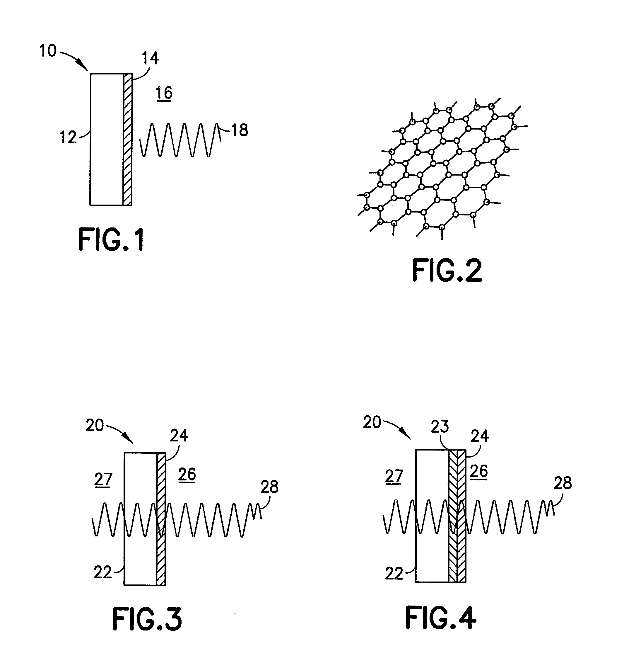
[0073]FIG. 1 illustrates a representation of a component 10 according to a first embodiment. The component 10 includes a multipactor-inhibiting carbon nanofilm 14 covering at least one surface 12 of the component 10, wherein a SEE coefficient of the multipactor inhibiting carbon nanofilm 14 is less than a SEE coefficient of the underlying surface 12 of the component 10 and, preferably, less than a SEE coefficient of conventional multipactor-inhibiting TiN coatings, which is approximately 1.5. In addition to the low SEE coefficient, the multipactor-inhibiting carbon nanofilm 14 has a low loss tangent to limit losses and overheating, and mechanical properties sufficient to handle extreme heating cycles under an applied vacuum load.

[0074]Since the SEE coefficient is a surface-sensitive property, the susceptibility of the component 10 to multipactor flashover will be controlled by the multipactor-inhibiting carbon nanofilm 14 rather than the underlying surface 12 of the component 10 if ...

second embodiment

[0082]The RF / microwave community has long identified RF windows as a major fault point, with frequent failure events due to multipactor flashover, putting a low upper limit on practical operating ranges. To address this need, the second embodiment is directed to improved RF windows having multipactor-inhibiting carbon nanofilms thereon.

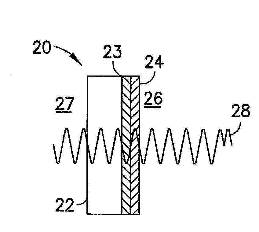
[0083]FIG. 3 illustrates a representation of an RF window 20 according to the second embodiment. An RF window is a conventional component of a high power RF (Radio Frequency) energy device, such as plasma sources, high power microwave devices and particle accelerating devices that require isolated vacuum environments in order to operate. Radio Frequency electron beam accelerators, klystrons, and magnetrons are all believed to require RF windows. As represented in FIG. 3, the RF window 20 includes a microwave transparent material 22 and a multipactor-inhibiting carbon nanofilm 24 covering at least one surface of the microwave transparent material 22.

[0...

third embodiment

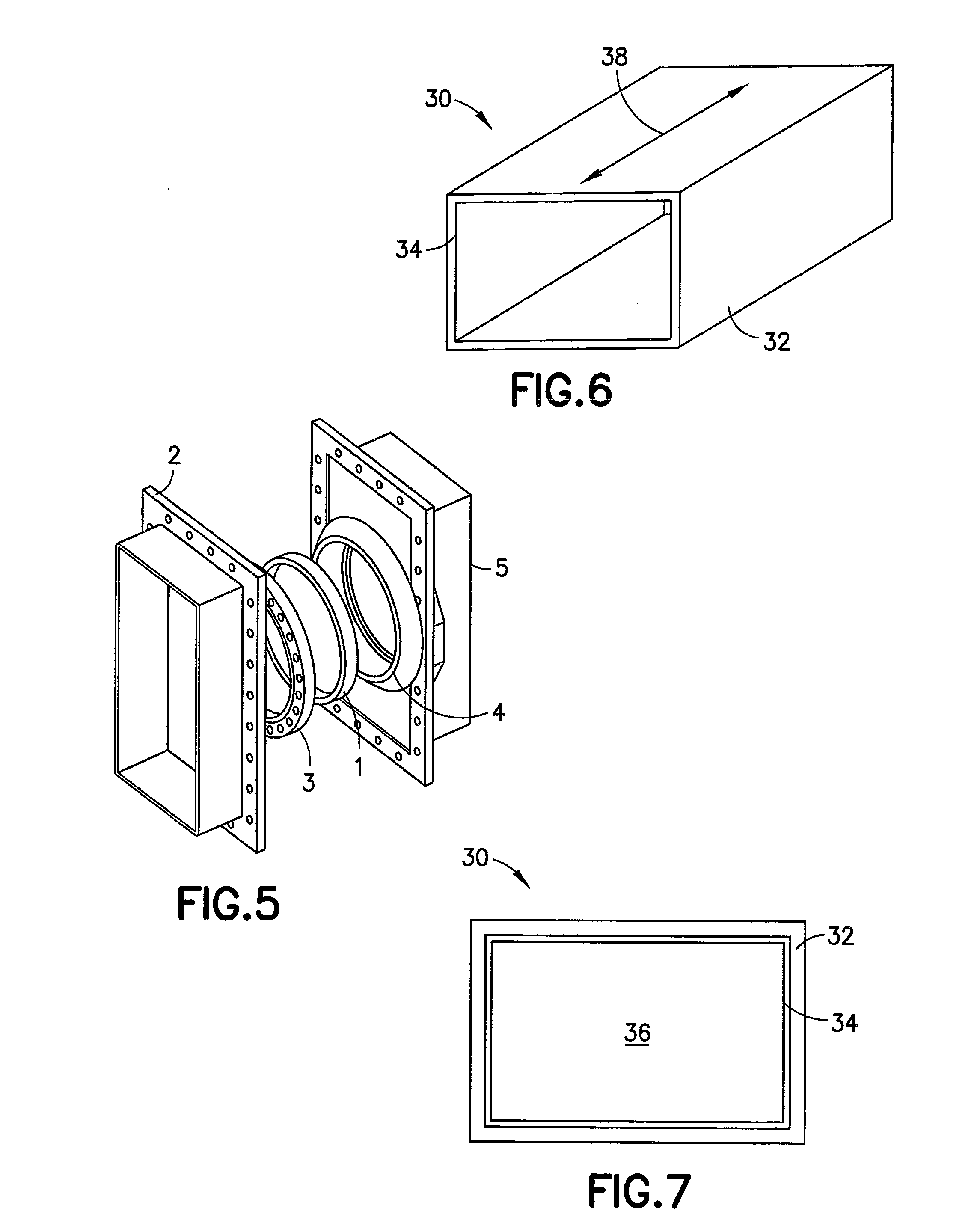
[0091]The RF / microwave community has also long strived to increase the power handling capability of waveguides in a vacuum. Waveguides for a high power RF energy device are typically used to channel energy and to filter frequencies. Many RF electron beam accelerators, klystrons, and magnetrons require such a waveguide. In order to guide energy generated from high power RF energy devices, waveguides include cavities that are put under a vacuum and exposed to high microwave energy. To address this need, the third embodiment is directed to improved waveguides having multipactor-inhibiting carbon nanofilms thereon.

[0092]As referenced herein, the term waveguide is used to include one or more structures that include one or more surfaces defining at least one cavity through which high power RF energy is guided. As shown in FIGS. 6 and 7, an illustrated waveguide 30 includes a plurality of surfaces 32 defining a cavity 36 through which high power RF energy is guided along a waveguide axis d...


PUM

PropertyMeasurementUnit
Thicknessaaaaaaaaaa
Thicknessaaaaaaaaaa
Thicknessaaaaaaaaaa

Abstract

A high power RF energy device component is disclosed that is exposed to high power RF energy in a vacuum environment, and includes a multipactor-inhibiting carbon nanofilm covering at least one surface of the component. A secondary electron efficiency (SEE) coefficient of the multipactor inhibiting carbon nanofilm is desirably less than a SEE coefficient of the underlying surface of the component.

Description

CROSS REFERENCE TO RELATED APPLICATIONS[0001]This application is based upon U.S. Provisional Patent Application No. 61 / 574,532 entitled “Structure for Inhibiting Multipactor in RF Devices and Method for Preparing the Same”, filed Aug. 4, 2011, which is hereby incorporated by reference for all purposes as if set forth herein.BACKGROUND OF THE INVENTION[0002]1. Field of the Invention[0003]The present invention relates to components having multipactor-inhibiting coatings for use in any circumstances where the phenomenon of multipactor flashover occurs. For example, such components may be provided to high power RF energy devices, such as plasma sources, microwave devices, particle accelerating devices that generate high power, low frequency energy corresponding to radio frequency, microwave, or millimeter wavelengths, and that require an isolated vacuum environment in order to operate. These components may be components of klystrons, Inductive Output Tubes (IOTs), linear accelerators, m...

Claims


Application Information

Patent Timeline
IPC IPC(8): H01P1/08H01J25/76H01J9/02B82Y99/00
CPCH01J23/36H01J23/12Y10T29/49002B82Y30/00B82Y40/00H01P1/08H01J25/76Y10T428/25Y10T428/30
Inventor FISHER, PATRICK J.KELLER, III, WALTER J.
Owner NOKOMIS
Why Eureka
Try Eureka