

Copper alloy for electronic device, method for producing copper alloy for electronic device, and copper alloy rolled material for electronic device
- Summary
- Abstract
- Description
- Claims
- Application Information
AI Technical Summary
Benefits of technology
Problems solved by technology
Method used
Image

Examples
first embodiment
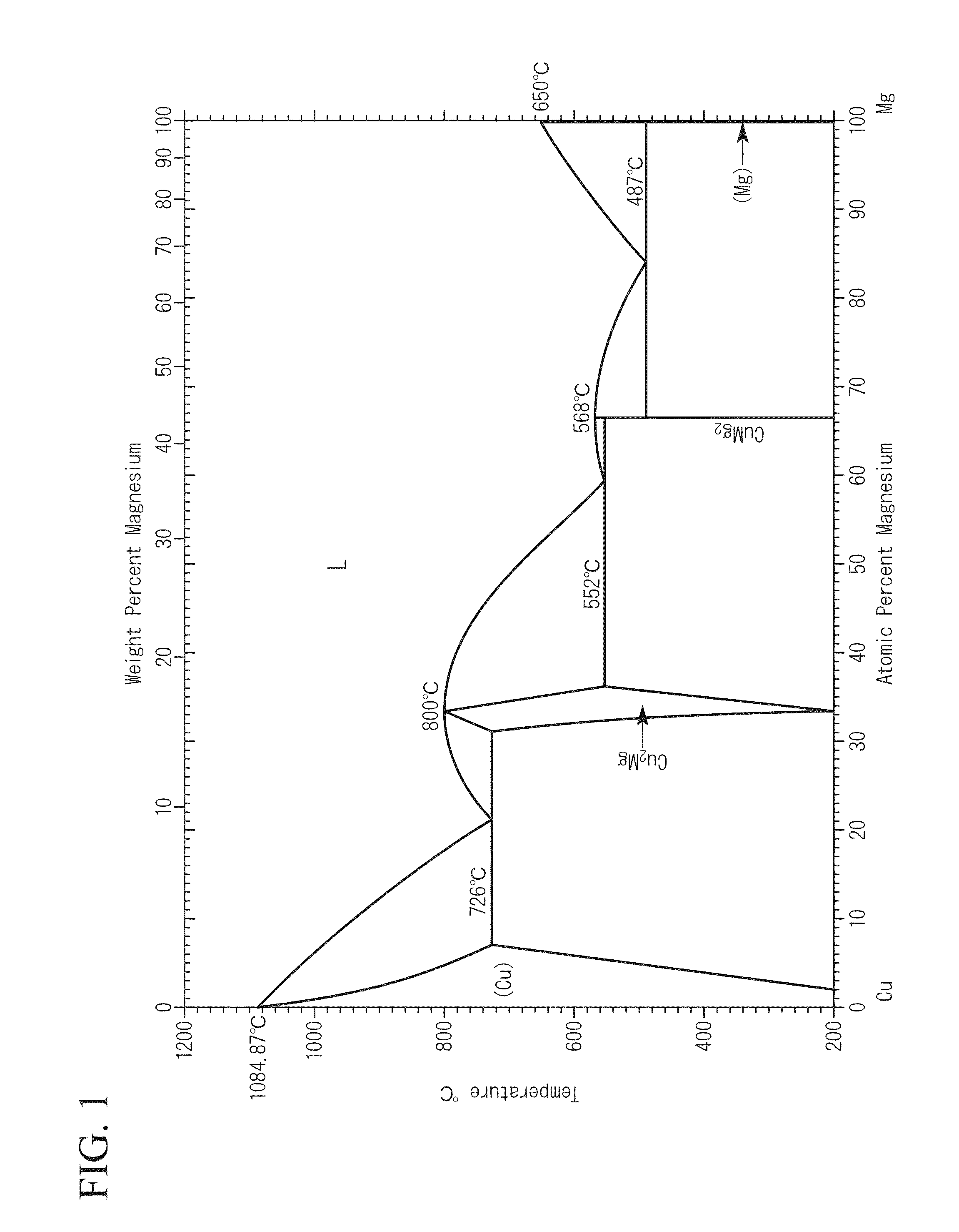
[0074]A copper alloy for an electronic device according to this embodiment is composed of a binary alloy of Cu and Mg. The binary alloy contains Mg at a content in a range of 3.3 to 6.9 atomic %, with a remainder being Cu and inevitable impurities.
[0075]A conductivity σ (% IACS) is within the following range when the content of Mg is given as A atomic %.
σ≦{1.7241 / (−0.0347×A2+0.6569×A+1.7)}×100
[0076]An average number of intermetallic compounds having grain sizes of 0.1 μm or more is in a range of 1 μm2 or less, and the average number is measured by observation using a scanning electron microscope.
[0077]A Young's modulus E of the copper alloy for an electronic device is in a range of 125 GPa or less, and a 0.2% proof stress σ0.2 is in a range of 400 MPa or more.
[0078](Composition)
[0079]Mg is an element having effects of improving a strength and raising a recrystallization temperature without greatly decreasing a conductivity. In addition, when Mg is dissolved in a matrix phase, the Yo...
second embodiment
[0134]A copper alloy for an electronic device of this embodiment is composed of a ternary alloy of Cu, Mg, and Zn. The ternary alloy contains Mg at a content in a range of 3.3 to 6.9 atomic %, and Zn at a content in a range of 0.1 to 10 atomic %, with a remainder being Cu and inevitable impurities.
[0135]When the content of Mg is given as A atomic % and the content of Zn is given as B atomic %, a conductivity a (% IACS) is within the following range.
σ≦{1.7241 / (X+Y+1.7)}×100
X=−0.0347×A2+0.6569×A
Y=−0.0041×B2+0.2503×B
[0136]An average number of intermetallic compounds having grain sizes of 0.1 μM or more in a range of 1 / μm2 or less, and the average number is measured by observation using a scanning electron microscope.
[0137]A Young's modulus E of the copper alloy for an electronic device is in a range of 125 GPa or less, and a 0.2% proof stress σ0.2 is in a range of 400 MPa or more.
[0138](Composition)
[0139]Mg is an element having effects of improving a strength and raising a recrystall...
example 1
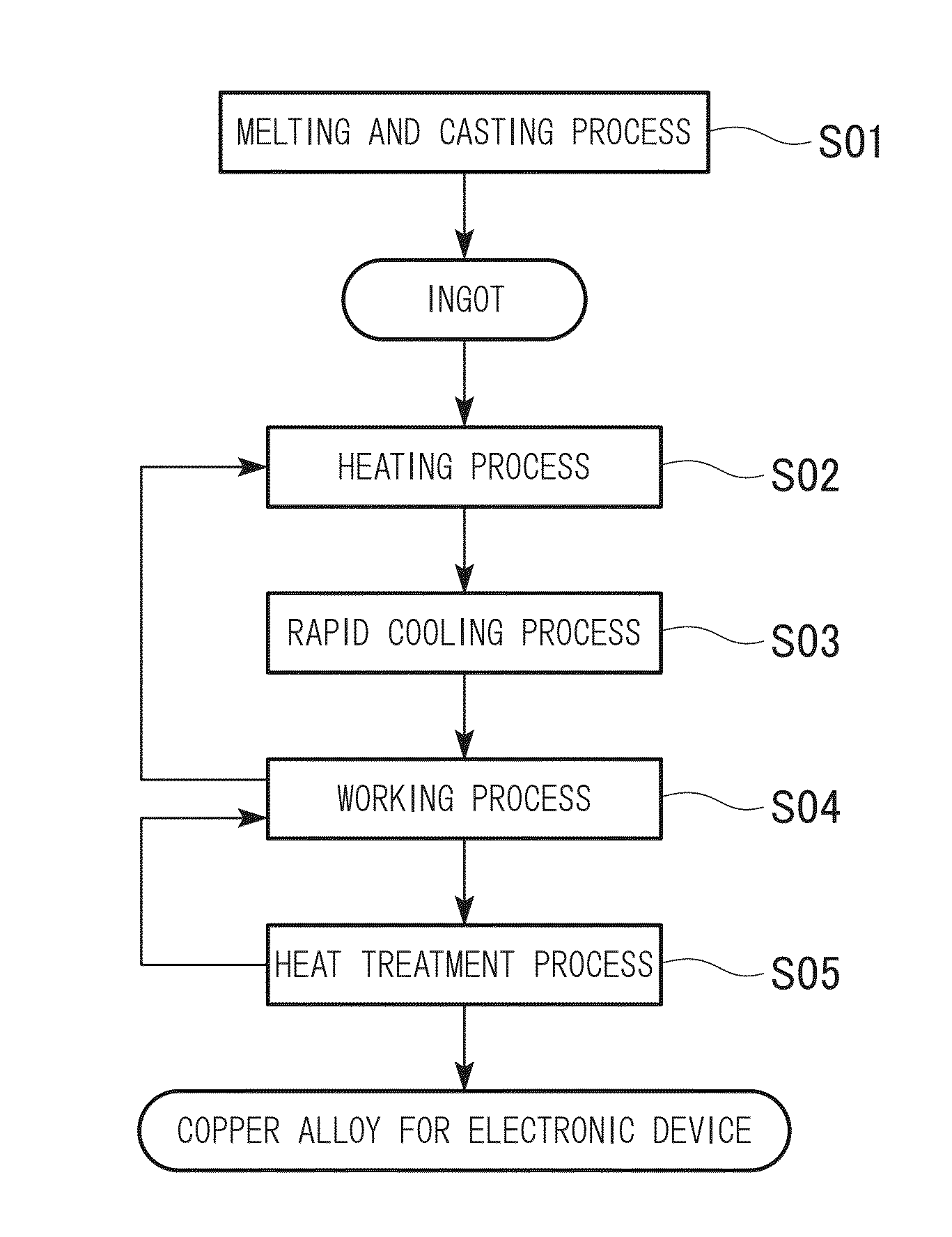
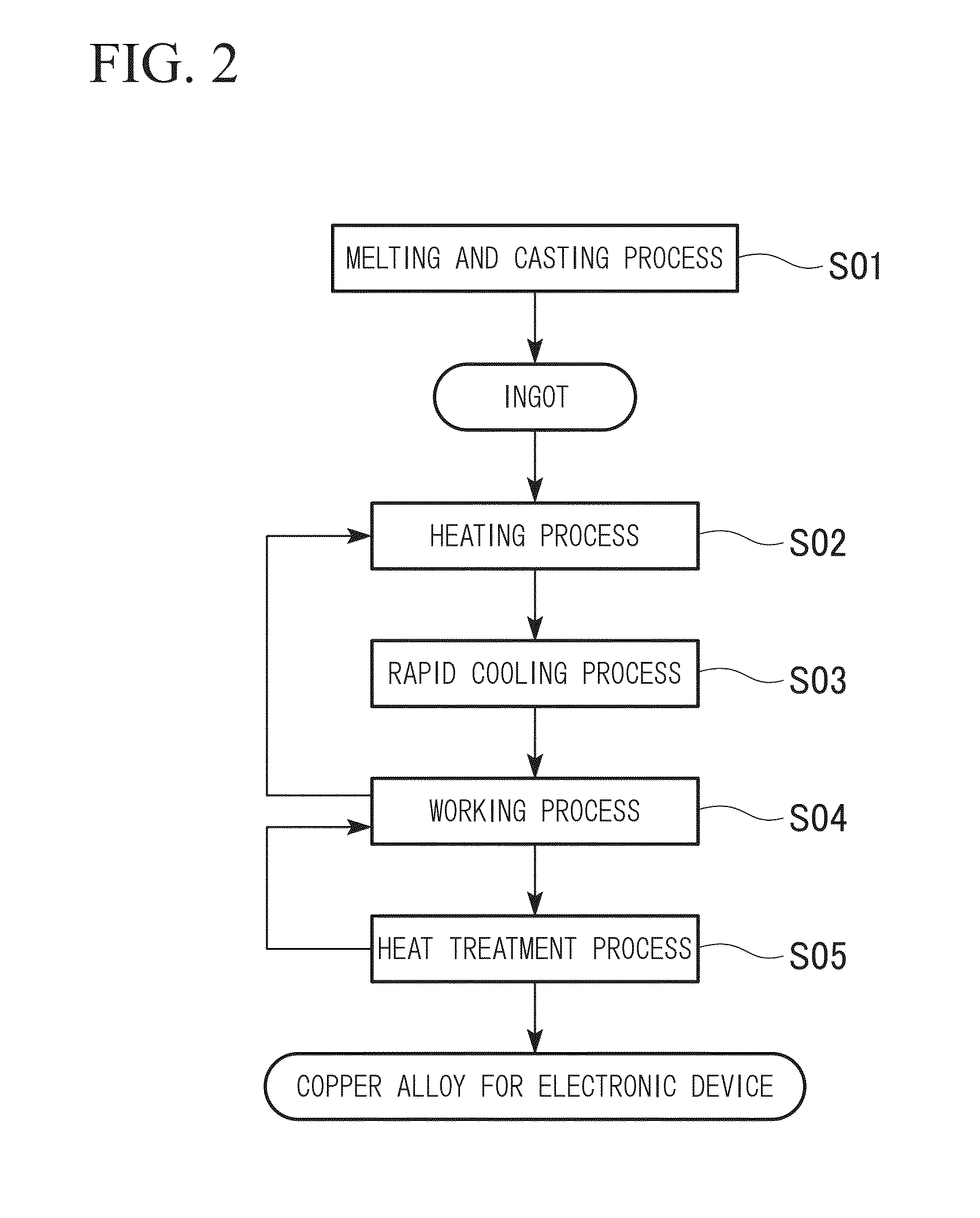
[0201]A copper raw material composed of oxygen-free copper (ASTM B152 C10100) having a purity of 99.99% by mass or more was prepared. This copper raw material was charged in a high purity graphite crucible, and the copper raw material was melted using a high frequency heater in an atmosphere furnace having an Ar gas atmosphere. Various elements were added to the molten copper so as to prepare component compositions shown in Table 1. Each of the resultant materials was poured into a carbon casting mold to produce an ingot. Here, the size of the ingot was set to have a thickness of approximately 20 mm×a width of approximately 20 mm×a length of approximately 100 to 120 mm. In addition, the remainder of the component composition shown in Table 1 was copper and inevitable impurities.
[0202]Each of the obtained ingots was subjected to a heating process of heating for four hours under a temperature condition described in Table 1, and then water quenching was performed.
[0203]The ingots after...
PUM
| Property | Measurement | Unit |
|---|---|---|
| Temperature | aaaaa | aaaaa |
| Temperature | aaaaa | aaaaa |
| Length | aaaaa | aaaaa |
Abstract
Description
Claims
Application Information