Copper alloy for electronic devices, method for producing copper alloy for electronic devices, copper alloy plastic working material for electronic devices, and component for electronic devices

A technology for electronic equipment and plastic processing, which is applied in the manufacturing of conductive materials, conductive materials, cables/conductors, etc. It can solve problems such as inability to form connectors, and achieve the effects of not easy plastic deformation, improved workability, and high elastic energy modulus.

Active Publication Date: 2014-01-08
MITSUBISHI MATERIALS CORP
View PDF14 Cites 9 Cited by
  • Summary
  • Abstract
  • Description
  • Claims
  • Application Information

AI Technical Summary

Problems solved by technology

Therefore, there is a problem that it is impossible to mold complex-shaped components for electronic devices such as connectors

Method used


Image

  • Copper alloy for electronic devices, method for producing copper alloy for electronic devices, copper alloy plastic working material for electronic devices, and component for electronic devices
  • Copper alloy for electronic devices, method for producing copper alloy for electronic devices, copper alloy plastic working material for electronic devices, and component for electronic devices
  • Copper alloy for electronic devices, method for producing copper alloy for electronic devices, copper alloy plastic working material for electronic devices, and component for electronic devices

Examples


no. 1 Embodiment approach )

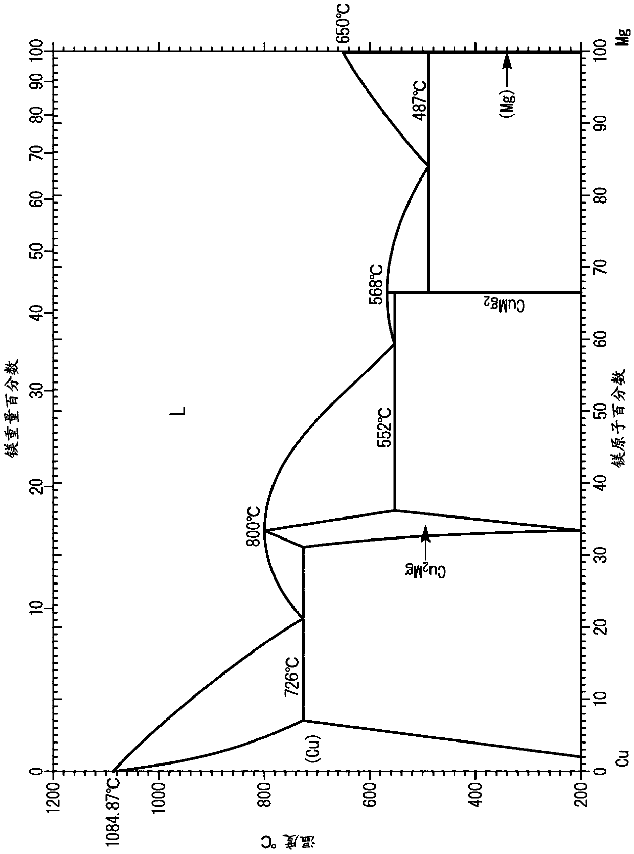
[0092] The copper alloy for electronic devices according to this embodiment contains Mg in a range of 3.3 atomic % to less than 6.9 atomic %, and contains at least either or both of Cr and Zr in a range of 0.001 atomic % to 0.15 atomic %. species, and the remainder is Cu and unavoidable impurities.

[0093] In addition, when the concentration of Mg is defined as A atomic %, the electrical conductivity σ(%IACS) satisfies the following formula (1).

[0094] σ≤{1.7241 / (-0.0347×A 2 +0.6569×A+1.7)}×100...(1)

[0095] In addition, the Young's modulus E of the copper alloy for electronic devices is 125 GPa or less, and the 0.2% yield strength σ 0.2 It is above 400MPa.

[0096] (composition)

[0097] Mg is an element that has the effect of increasing the strength and increasing the recrystallization temperature without greatly reducing the electrical conductivity. Furthermore, by making Mg solid-solubilized in the matrix, the Young's modulus is kept low and excellent bending work...

no. 2 Embodiment approach )

[0155] The composition of the copper alloy for electronic devices according to the present embodiment contains Mg in the range of 3.3 atomic % to 6.9 atomic %, and at least either of Cr and Zr in the range of 0.001 atomic % to 0.15 atomic %, respectively. or two, and the remainder is Cu and unavoidable impurities.

[0156] In addition, when the content of Mg is represented as X atomic %, the electrical conductivity σ (%IACS) satisfies the following formula (2).

[0157] σ≤{1.7241 / (-0.0347×X 2 +0.6569×X+1.7)}×100...(2).

[0158] In addition, the average number of intermetallic compounds mainly composed of Cu and Mg with a particle size of 0.1 μm or more observed by a scanning electron microscope was 1 piece / μm 2 the following.

[0159] In addition, the stress relaxation rate at 150° C. for 1000 hours is 50% or less. Here, the stress relaxation rate was measured by applying a stress by a method based on the cantilever thread type of JCBA-T309:2004 of the Japan Copper Associa...

Embodiment 1)

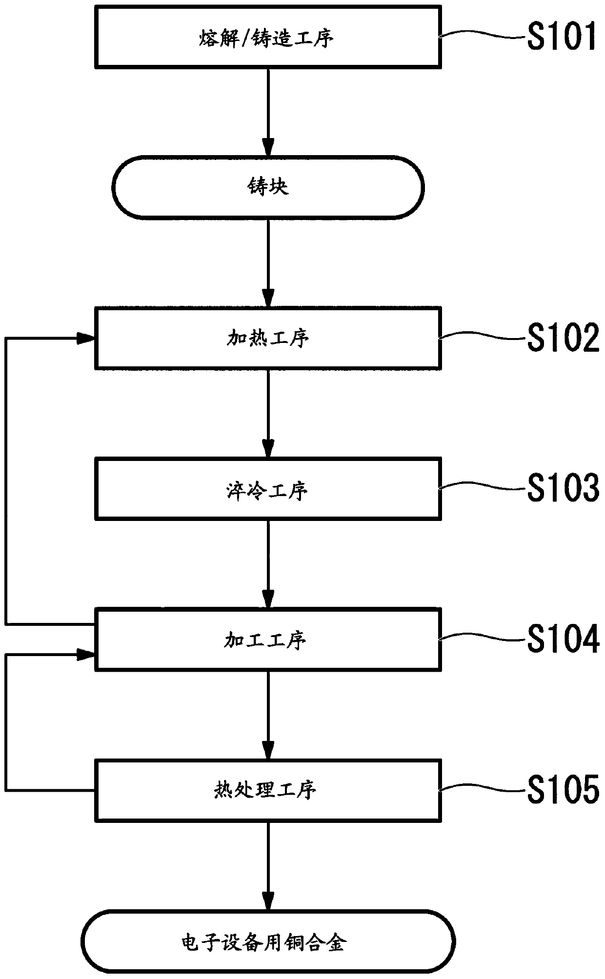
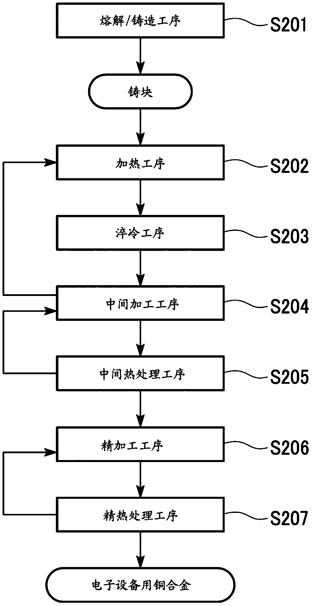
[0259] A copper raw material composed of oxygen-free copper (ASTM B152C10100) with a purity of 99.99% by mass or higher was prepared. This copper raw material was put into a high-purity graphite crucible, and high-frequency melting was carried out in an atmosphere furnace set as an Ar gas atmosphere to obtain molten copper. Various additive elements were added to the obtained molten copper to prepare the component compositions shown in Tables 1 and 2, and cast into a carbon mold to manufacture ingots. In addition, the size of the ingot was about 20 mm in thickness x about 30 mm in width x about 100 to 120 mm in length. In addition, in the compositions shown in Tables 1 and 2, the remainder other than Mg, Cr, and Zr is Cu and unavoidable impurities.

[0260] The obtained ingot was subjected to a heating step (homogenization / solutionization) under the temperature conditions described in Tables 1 and 2 in an Ar gas atmosphere for 4 hours, and then water quenched.

[0261] The h...


PUM

PropertyMeasurementUnit
yield strengthaaaaaaaaaa
crystal sizeaaaaaaaaaa
yield strengthaaaaaaaaaa

Abstract

One embodiment of this copper alloy contains Mg in an amount within the range from 3.3% by atom (inclusive) to 6.9% by atom (exclusive) and Cr and / or Zr respectively in an amount within the range from 0.001% by atom (inclusive) to 0.15% by atom (inclusive), with the balance made up of Cu and unavoidable impurities. When the Mg concentration is represented by A% by atom, the electrical conductivity s (% IACS) satisfies the following formula (1). s = {1.7241 / (-0.0347 × A2 + 0.6569 × A + 1.7)} × 100 (1) One embodiment of this method for producing a copper alloy comprises: a step wherein a copper material having the composition of the above-described copper alloy is heated to a temperature within the range from 300°C to 900°C (inclusive); a step wherein the heated copper material is quenched to 200°C or less at a cooling rate of 200°C / min or more; and a step wherein the quenched copper material is worked.

Description

technical field [0001] The present invention relates to a copper alloy for electronic equipment suitable for components (electrical and electronic components) such as terminals, connectors, relays, and lead frames for electronic equipment, a method for manufacturing copper alloy for electronic equipment, and plastic processing of copper alloy for electronic equipment materials, and components for electronic equipment. [0002] This application claims priority based on Japanese Patent Application No. 2011-126510 filed in Japan on June 6, 2011, and Japanese Patent Application No. 2011-243870 filed in Japan on November 7, 2011, the contents of which are cited in in this manual. Background technique [0003] Conventionally, with the miniaturization of electronic equipment and electrical equipment, etc., components for electronic equipment (electrical and electronic components) such as terminals, connectors, relays, and lead frames used in these electronic equipment and electric...

Claims


Application Information

Patent Timeline
Patent Type & Authority Applications(China)
IPC IPC(8): C22C9/00B21B3/00C22F1/08H01B1/02H01B13/00C22F1/00
CPCH01B1/026C22F1/08C22C9/00
Inventor 牧一诚伊藤优树
Owner MITSUBISHI MATERIALS CORP
Why Eureka
Try Eureka