20v to 250v high current ASIC pin diode driver

a pin diode driver, high current technology, applied in the direction of pulse generator, pulse technique, electric pulse generator circuit, etc., can solve the problems of pin driver use such a charge pump is not acceptable, pin driver use cannot be fully integrated, and pin driver use cannot be accepted

Active Publication Date: 2013-02-28
MACOM TECH SOLUTIONS HLDG INC
View PDF7 Cites 14 Cited by
  • Summary
  • Abstract
  • Description
  • Claims
  • Application Information

AI Technical Summary

Benefits of technology

[0006]The objects, features and advantages of the present invention include providing a method and/or apparatus for implementing a high voltage, high current application specific integrated circuit (ASIC) PIN diode driver that may (i) be fully integrated, (ii) achieve a desired current capability without external power MOSFETs, (iii) provide 200 mA current to two independent series diodes and 50 mA current to two independent shunt diodes, (iv) drive a typical series/shunt, series/shunt SPDT PIN diode switch, (v) be extended to drive switches of any number of poles and throws, (vi) be extended to drive absorptive, as ...

Problems solved by technology

Currently, no fully integrated high voltage PIN diode driver exists.
Commercially available full-bridge or half-bridge gate driver ICs cannot be used because bootstrap capacitors are required to form a charge pump to fully shut down ...

Method used


Image

  • 20v to 250v high current ASIC pin diode driver
  • 20v to 250v high current ASIC pin diode driver
  • 20v to 250v high current ASIC pin diode driver

Examples


Embodiment Construction

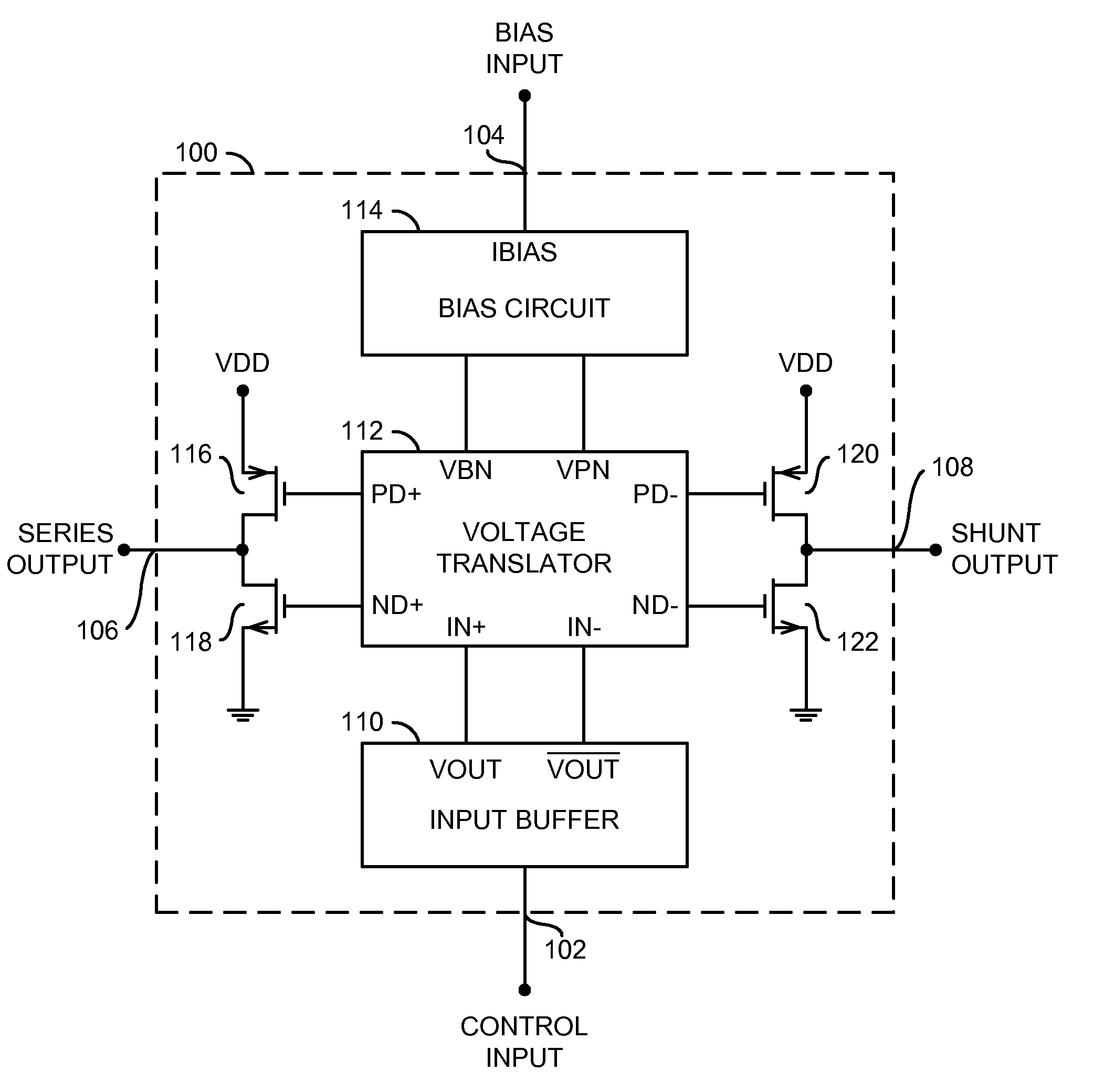
[0017]The present invention generally provides a fully integrated solution to drive high power PIN diodes. The fully integrated solution may be utilized in applications that involve both high sinking current capability and high voltage back biasing to provide enough isolation. For example, a fully integrated PIN diode driver circuit implemented in accordance with an embodiment of the present invention may be utilized in commercial and / or military radio frequency (RF) applications (e.g., communications, etc.).

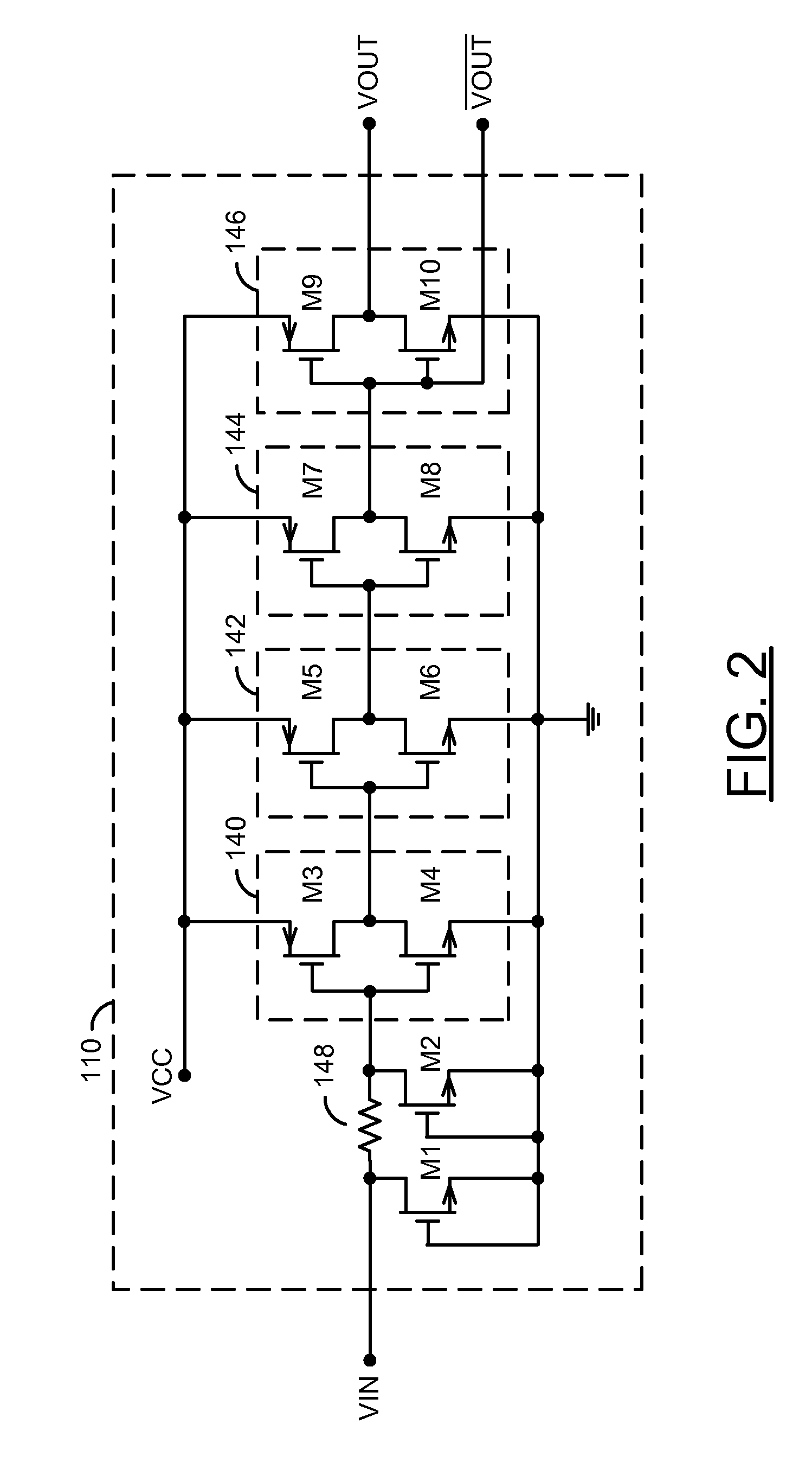
[0018]Referring to FIG. 1, a block diagram of a circuit 100 is shown illustrating a high current application specific integrated circuit (ASIC) PIN diode driver in accordance with a example embodiment of the present invention. In one example, the circuit 100 may have an input 102 that may receive a signal (e.g., CONTROL INPUT), an input 104 that may receive a signal (e.g., BIAS INPUT), a first output 106 that may present a signal (e.g., SERIES OUTPUT) and an output 108 that may ...


PUM


Abstract

An integrated circuit including a first circuit, a second circuit, a third circuit, a first complementary pair of transistors, and a second complementary pair of transistors. The first circuit may be configured to generate a first input signal in response to a first control input signal. The second circuit may be configured to generate a first output signal and a second output signal in response to the first input signal and a bias signal. The third circuit may be configured to generate the bias signal in response to a bias input signal. The first complementary pair of transistors may be configured to drive a first series output of the integrated circuit in response to the first output signal. The second complementary pair of transistors may be configured to drive a first shunt output of the integrated circuit in response to the second output signal.

Description

[0001]This application claims the benefit of U.S. Provisional Application No. 61 / 525,982, filed Aug. 22, 2011, and is hereby incorporated by reference in its entirety.FIELD OF THE INVENTION[0002]The present invention relates to current drivers generally and, more particularly, to a method and / or apparatus for implementing a 20V to 250V high current application specific integrated circuit (ASIC) PIN diode driver.BACKGROUND OF THE INVENTION[0003]P Intrinsic N (PIN) diodes are used commonly in an assortment of commercial and military applications as switches, phase shifters, and attenuators. Currently, no fully integrated high voltage PIN diode driver exists. Instead, conventional systems use discrete power MOSFETs (metal-oxide-semiconductor field effect transistors) to achieve the bias current requirement for the high power PIN diodes. The discrete power MOSFETs limit a gate to source voltage to no higher than 20V to 25V. The gate to source voltage limitation requires the addition of ...

Claims


Application Information

Patent Timeline
IPC IPC(8): H03K3/021
CPCH03K3/356182H03K17/76H03K17/74
Inventor LIU, CHENGXINWEIGAND, CHRISTOPHER D.GIACCHINO, RICHARD J.VASQUEZ, SCOTT
Owner MACOM TECH SOLUTIONS HLDG INC
Why Eureka
Try Eureka