Carbon film laminate

Active Publication Date: 2013-02-28
NAT INST OF ADVANCED IND SCI & TECH
View PDF6 Cites 14 Cited by
  • Summary
  • Abstract
  • Description
  • Claims
  • Application Information

AI Technical Summary

Benefits of technology

The carbon film laminate in this patent allows for the production of larger crystal sizes of graphene, which was previously limited to several tens of μm. This allows for the production of ultrahigh performance electronic devices, such as graphene transistors, that were previously not possible. The laminate also allows for the integration of various performance devices, resulting in the creation of ultrahigh performance devices.

Problems solved by technology

To use graphene as a material in a high-performance electronic device or the like, there is a need for the graphene to have as large a crystal size as possible, and thus the issue is to increase the crystal size.

Method used


Image

  • Carbon film laminate
  • Carbon film laminate
  • Carbon film laminate

Examples


Embodiment Construction

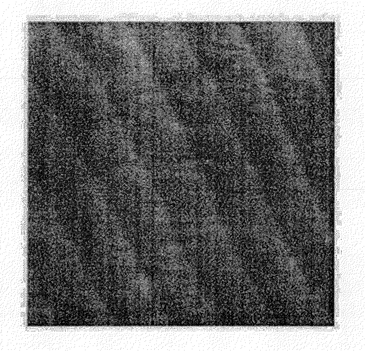
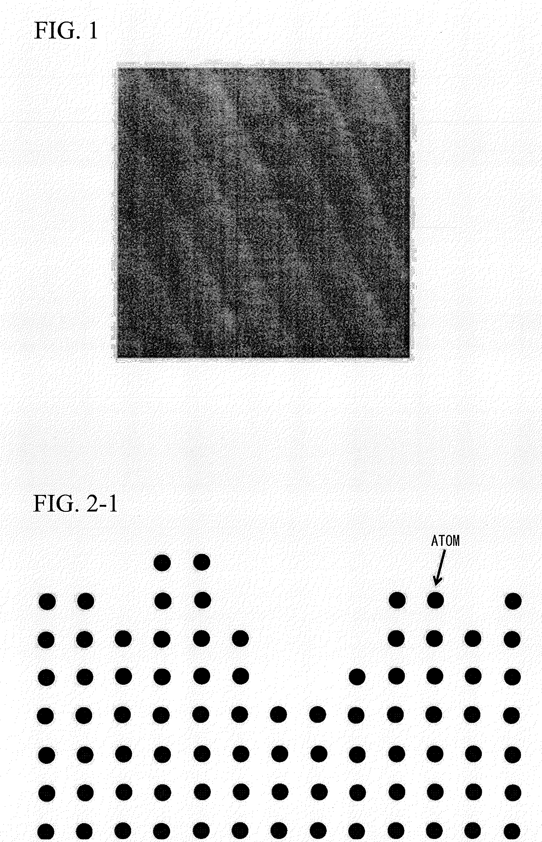
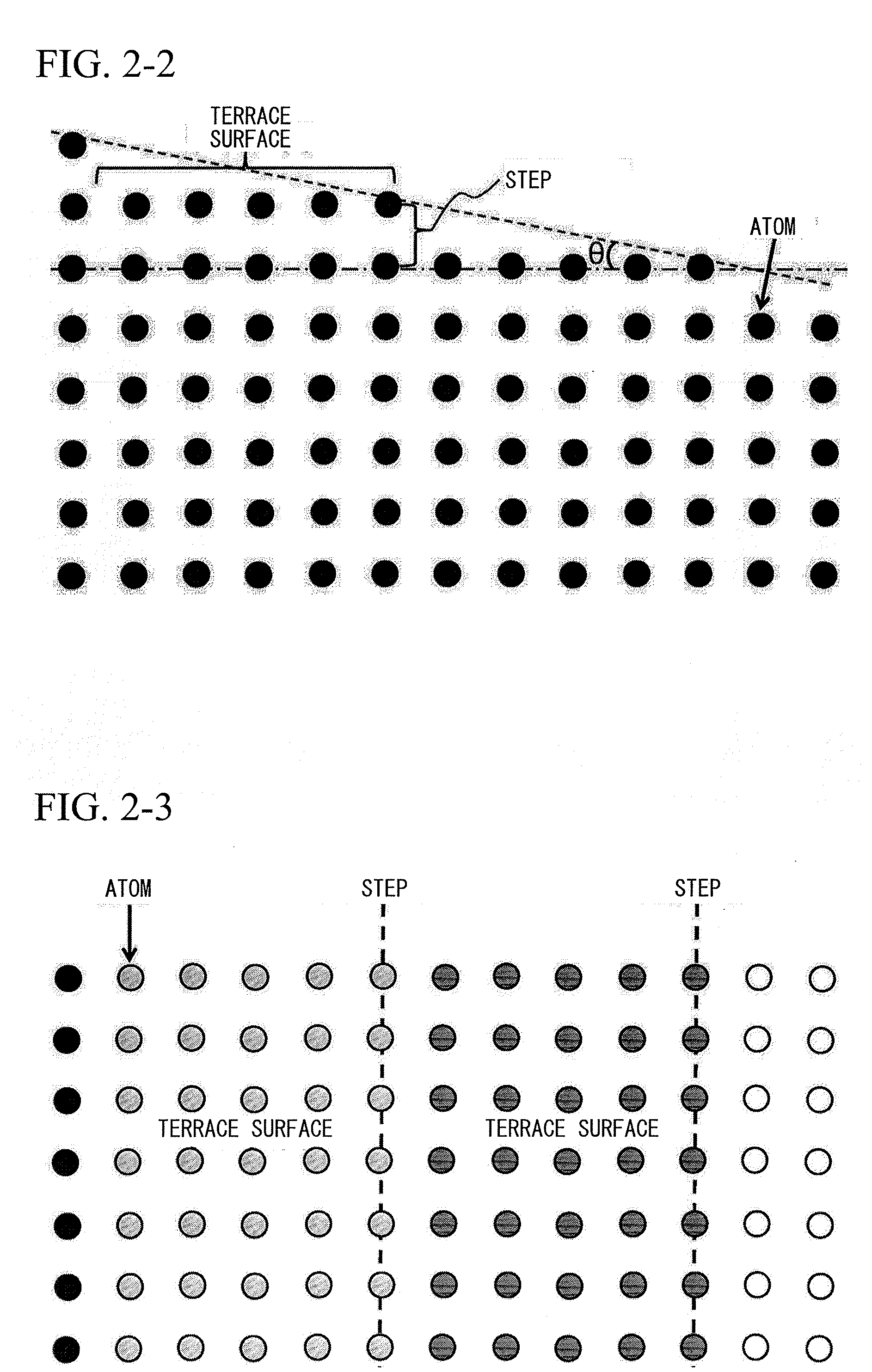
[0027]Graphene is a flat single layer carbon film composed of sp2-bonded carbon atoms. (Graphene is described in detail in Non-Patent Literature 1.) A carbon film laminate of the present invention in which graphene having a large crystal size is deposited is mainly provided based on the employment of specific production conditions. In the carbon film laminate in which graphene having a large crystal size is formed, a copper (111) single crystal thin film formed by epitaxial growth on a sapphire (0001) single crystal substrate is used as a base material for synthesis of graphene. It is also desired to select the concentration and mole ratio of raw gases, reaction time and the like as the production conditions by a thermal CVD method.

[0028]Before the present invention is described, formation of a film of graphene through thermal CVD was performed by the methods disclosed in Non-Patent Literatures 1 and 2 using a copper foil as a base material. Since the copper foil is a polycrystal, i...


PUM

PropertyMeasurementUnit
Pressureaaaaaaaaaa
Crystal sizeaaaaaaaaaa

Abstract

An object of the present invention is to solve a problem such as a small crystal size, which is the issue of a conventional method for formation of a film of graphene by a thermal CVD technique using a copper foil as a substrate, and thus providing a carbon film laminate in which graphene having a larger crystal size is formed. The carbon film laminate is configured to include a sapphire (0001) single crystal having a surface composed of terrace surfaces which are flat at the atomic level, and atomic-layer steps, a copper (111) single crystal thin film formed by epitaxial growth on the substrate and graphene deposited on the copper (111) single crystal thin film, and thus enabling formation of graphene having a large crystal size.

Description

TECHNICAL FIELD[0001]The present invention relates to a large area carbon film laminate for use in electronic devices, transparent conductive films and the like.BACKGROUND ART[0002]Graphene, which is in a form of a flat single layer carbon film composed of sp2-bonded carbon atoms, is expected to be used as a base material such as an ultrahigh performance electronic device and a transparent conductive thin film due to its specifically high electrical conductivity and optical transmittance. Heretofore, methods for formation of graphene have been developed, such as a method for peeling from natural graphite, a method for eliminating silicon by a high-temperature heat treatment of silicon carbide, a method for forming graphene on various metal surfaces and the like.[0003]In particular, a method for forming a single to several layers of graphene on a surface of a copper foil by a chemical vapor deposition (CVD) method has recently been developed (Non-Patent Literatures 1 and 2). The tech...

Claims


Application Information

Patent Timeline
IPC IPC(8): B32B15/20B32B33/00C01B31/00B32B15/04B32B9/04B82Y30/00C01B32/50
CPCB82Y30/00B82Y40/00C01B31/02C23C16/0281C23C16/26Y10T428/30C30B29/04C30B29/20C01B31/0453C01B31/20C30B29/02C01B32/05C01B32/186C01B32/50Y10T428/31678C01B32/19
Inventor HASEGAWA, MASATAKAISHIHARA, MASATOUKOGA, YOSHINORIKIM, JAEHOTSUGAWA, KAZUOIIJIMA, SUMIO
Owner NAT INST OF ADVANCED IND SCI & TECH
Why Eureka
Try Eureka