Method for Manufacturing Thin Film Transistor, Thin Film Transistor and Image Display Apparatus

a technology of thin film transistor and image display device, which is applied in the direction of optics, instruments, electroluminescent light sources, etc., can solve the problems of increasing manufacturing costs, reduce the number of manufacturing processes in manufacturing thin film transistors, and reduce the number of photolithography processes. , the effect of reducing the number of manufacturing processes

Inactive Publication Date: 2013-03-07
TOPPAN PRINTING CO LTD
View PDF3 Cites 7 Cited by
  • Summary
  • Abstract
  • Description
  • Claims
  • Application Information

AI Technical Summary

Benefits of technology

[0029]As the protection film is set to have a layered structure of an inorganic material and organic materials, it is possible to consecutively deposit the protection film formed of the inorganic material, after the film formation of the semiconductor layer. As a result, it is possible to lessen damage to the surface of the semiconductor layer in the manufacturing process.
[0030]In addition, according to the present invention, the protection film formed on the semiconductor layer is used as the mask when etching. As a result, since it is possible to reduce a photolithography process or the like for patterning the semiconductor layer, the number of the manufacturing processes in manufacturing the thin film transistor may be reduced and additionally the manufacturing may be simplified.
[0031]Herein, since an ink jet method is us

Problems solved by technology

The complicated manufacturing process

Method used


Image

  • Method for Manufacturing Thin Film Transistor, Thin Film Transistor and Image Display Apparatus
  • Method for Manufacturing Thin Film Transistor, Thin Film Transistor and Image Display Apparatus
  • Method for Manufacturing Thin Film Transistor, Thin Film Transistor and Image Display Apparatus

Examples


first embodiment

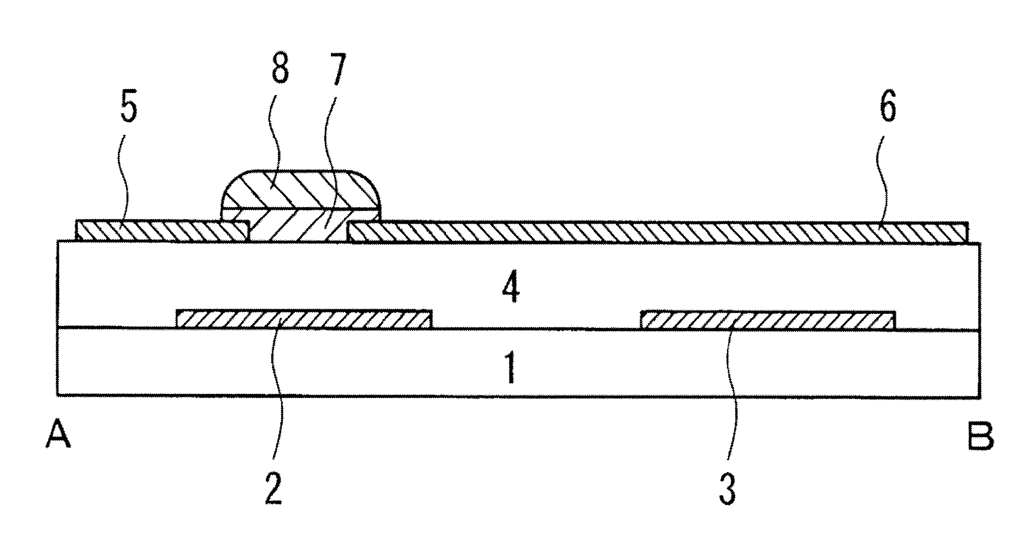
[0080]As a first embodiment based on the present invention, an active matrix substrate illustrated in FIG. 5 was manufactured.

[0081]As a substrate 1, an alkali-free glass EAGLE 2000 made by Corning Incorporated was used. ITO was deposited with a film thickness of 100 nm on the substrate 1 using a DC magnetron sputtering method and a patterning was performed for a desired shape using a photolithography method. More specifically, after applying a photosensitive positive photoresist, exposing and developing by alkaline developing agent was performed, and a resist pattern of a desired shape was formed. Etching was further performed using an ITO etching solution to dissolve the unnecessary ITO. Then, the photoresist was removed using a resist stripping solution and a gate electrode 2 and a capacitor electrode 3 of a desired shape were formed (hereinafter, such a patterning method is referred to as a photolithography method and omitted in description).

[0082]Next, on the entire surface oth...

second embodiment

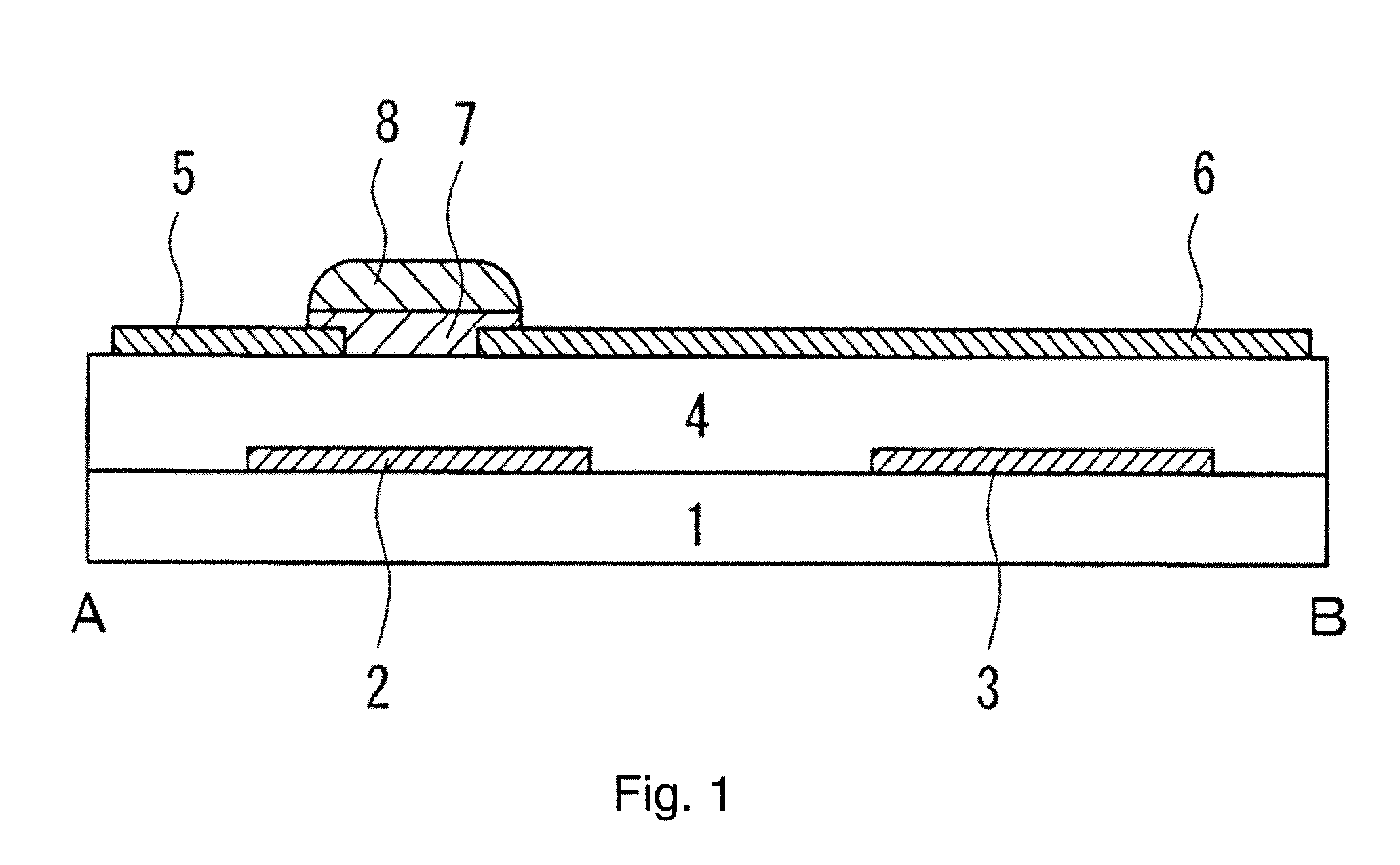
[0089]As a second embodiment based on the present invention, an active matrix substrate illustrated in FIG. 6 was manufactured.

[0090]As a substrate 1, an alkali-free glass eagle 2000 made by Corning Incorporated was used. ITO was deposited with a film thickness of 100 nm on the substrate 1 using a DC magnetron sputtering method and a patterning was performed for a desired shape using a photolithography method. More specifically, after applying a photosensitive positive photoresist, exposing and developing by alkaline developing agent were performed, and a resist pattern of a desired shape was formed. Etching was further performed using an ITO etching solution to dissolve the unnecessary ITO. Then, the photoresist was removed using a resist stripping solution and a gate electrode 2 and a capacitor electrode 3 of a desired shape were formed (hereinafter, such a patterning method is referred to as a photolithography method and omitted in description).

[0091]Next, on the entire surface o...

third embodiment

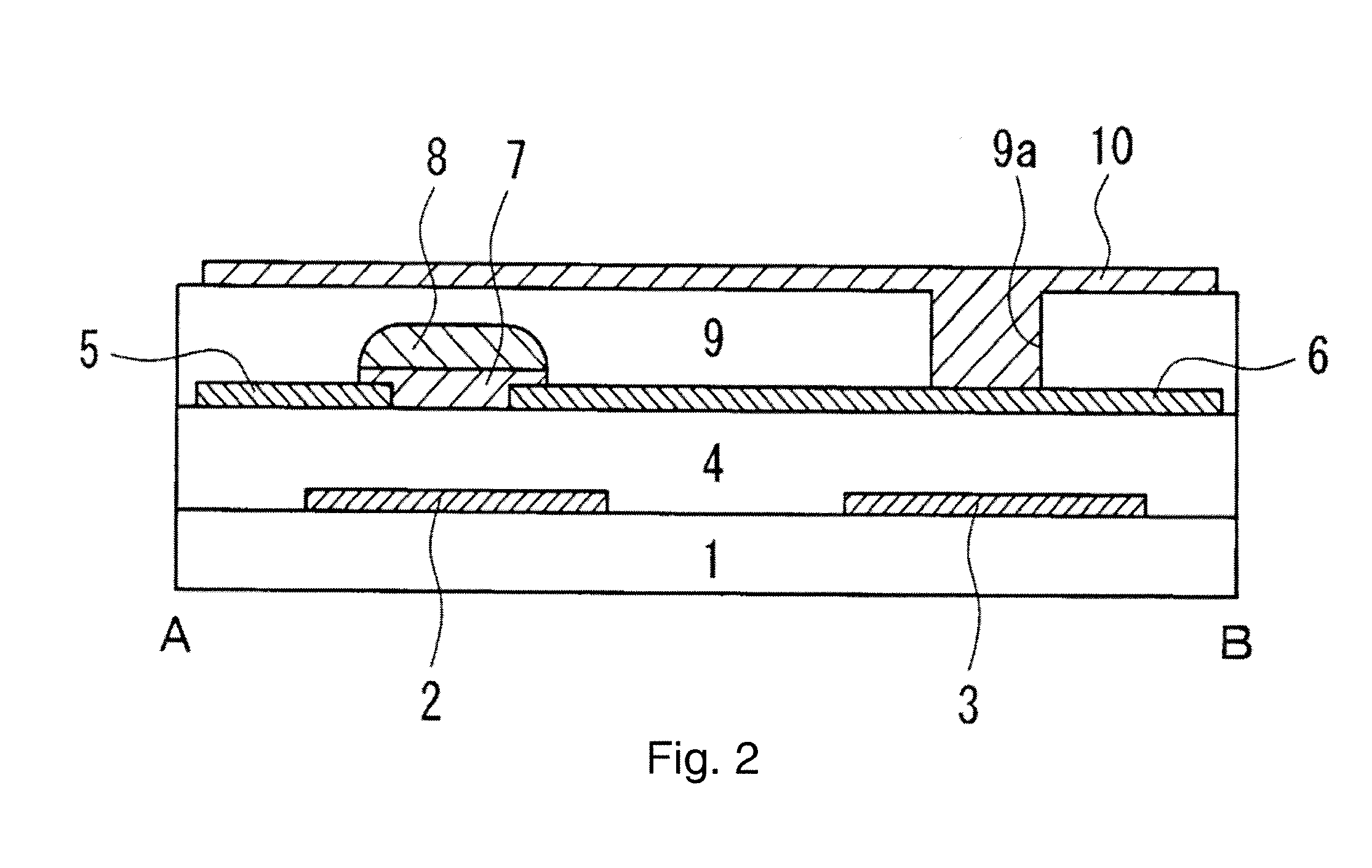
[0098]As a third embodiment based on the present invention, an active matrix substrate illustrated in FIG. 7 was manufactured.

[0099]As a substrate 1, an alkali-free glass EAGLE 2000 made by Corning Incorporated was used. ITO was deposited with a film thickness of 100 nm on the substrate 1 using a DC magnetron sputtering method and a patterning was performed for a desired shape using a photolithography method. More specifically, after applying a photosensitive positive photoresist, exposing and developing by alkaline developing agent were performed, and a resist pattern of a desired shape was formed. Etching was further performed using an ITO etching solution to dissolve the unnecessary ITO. Then, the photoresist was removed using a resist stripping solution and a gate electrode 2 and a capacitor electrode 3 of a desired shape were formed (hereinafter, such a patterning method is referred to as a photolithography method and omitted in description).

[0100]Next, on the entire surface ot...


PUM


Abstract

A method for manufacturing a thin film transistor includes a first process of forming a gate electrode on a substrate; a second process of forming a gate insulation film so as to cover the gate electrode; a third process of forming a source electrode and a drain electrode on the gate insulation film; a fourth process of forming a semiconductor layer connected to the source electrode and the drain electrode; a fifth process of forming a protection film so as to overlap a portion of the source electrode and the drain electrode immediately above the semiconductor layer; and a sixth process of patterning the semiconductor layer using the protection film as a mask.

Description

CROSS-REFERENCE TO RELATED APPLICATION[0001]This application is a continuation of International Application No. PCT / JP2011 / 054639, filed Mar. 1, 2011, which is incorporated herein by reference.BACKGROUND OF THE INVENTION[0002]1. Field of the Invention[0003]The present invention relates to a technology characterized in a thin film transistor which is used in an image display apparatus, an active matrix substrate and the like, and a manufacturing method of the thin film transistor.[0004]2. Background Art[0005]In recent years, as the image display apparatus, an image display apparatus such as a liquid crystal display apparatus, an electrophoresis display apparatus and an organic electroluminescence display apparatus which applies an active matrix substrate configured of the thin film transistor thereto has been widely used.[0006]In the image display apparatus which applies the active matrix substrate thereto, as disclosed in JP-B-8-16757, amorphous silicon or polycrystalline silicon is...

Claims


Application Information

Patent Timeline
IPC IPC(8): H01L33/08H05B44/00
CPCG02F1/1368H01L29/66765H01L27/1225H01L27/1248H01L27/124H01L29/78696
Inventor IKEDA, NORIAKIIMAMURA, CHIHIROITO, MANABU
Owner TOPPAN PRINTING CO LTD
Why Eureka
Try Eureka