
Soi integrated circuit comprising adjacent cells of different types

a technology of integrated circuits and adjacent cells, applied in the field of integrated circuits, can solve problems such as and the inability to meet the requirements of the application

Active Publication Date: 2013-03-14
COMMISSARIAT A LENERGIE ATOMIQUE ET AUX ENERGIES ALTERNATIVES +1
View PDF3 Cites 47 Cited by
  • Summary
  • Abstract
  • Description
  • Claims
  • Application Information

AI Technical Summary

Benefits of technology

The patent describes an invention relating to an integrated circuit with logic gates and memory cells. The invention addresses issues such as poor performance and high power consumption in previous circuits. The technical effects of the invention include the use of different materials and doping techniques for the logic gates and memory cells, resulting in improved performance, reduced power consumption, and the use of a biasing circuit for the ground planes of the transistors. The integrated circuit also includes a circuit for dynamically modifying the biasing of the ground planes of the transistors. Overall, the invention provides a more efficient and effective integrated circuit for high performance applications.

Problems solved by technology

However, the use of novel materials and / or novel architectures generally leads to difficulties of manufacture and / or problems of reliability of the integrated circuit.
Similarly, the use of a novel type of transistor entails problems in terms of portability and compatibility of the already existing circuits as well as the circuit techniques used to improve performance.
It is generally noted that SOI integrated circuits are less sensitive to the effects of ionizing radiation and hence prove to be more reliable in applications where such radiation can give rise to operational problems, especially in space applications.
However, in FDSOI (Fully Depleted Silicon-On-Insulator) technology, the doping of the channel is almost zero.
Thus, the channel doping level in the transistors cannot show major variations without losing the associated advantages, and this fact makes it impossible to differentiate the threshold voltages by bringing this doping into play.
The designing of such functions of the circuit proves to be relatively difficult because additional designing constraints have to be taken into account. FIGS. 1a to 1c provide an example of pairs of nMOS and pMOS transistors of different types, namely HVT, SVT and LVT types respectively.
The process of implanting dopants in the structure leads to undesirable variations in concentration at the edge of the implantations, inducing undesirable doping of the channel of the transistors.
At the scale of the integrated circuits used, these variations take the form of effects known as WPE (well proximity effects) that are not negligible and affect the reliability and efficiency of manufacture of such circuits.
The use of different gate materials also has non-negligible consequences on the complexity of the manufacturing process and its efficiency, especially as the integrated circuit has high density.

Method used


Image

  • Soi integrated circuit comprising adjacent cells of different types
  • Soi integrated circuit comprising adjacent cells of different types
  • Soi integrated circuit comprising adjacent cells of different types

Examples


Embodiment Construction

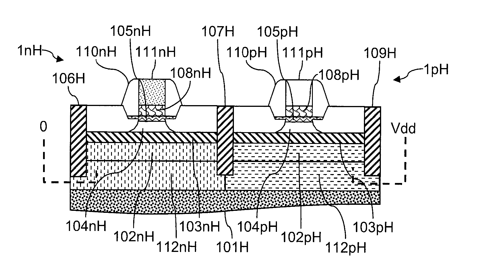
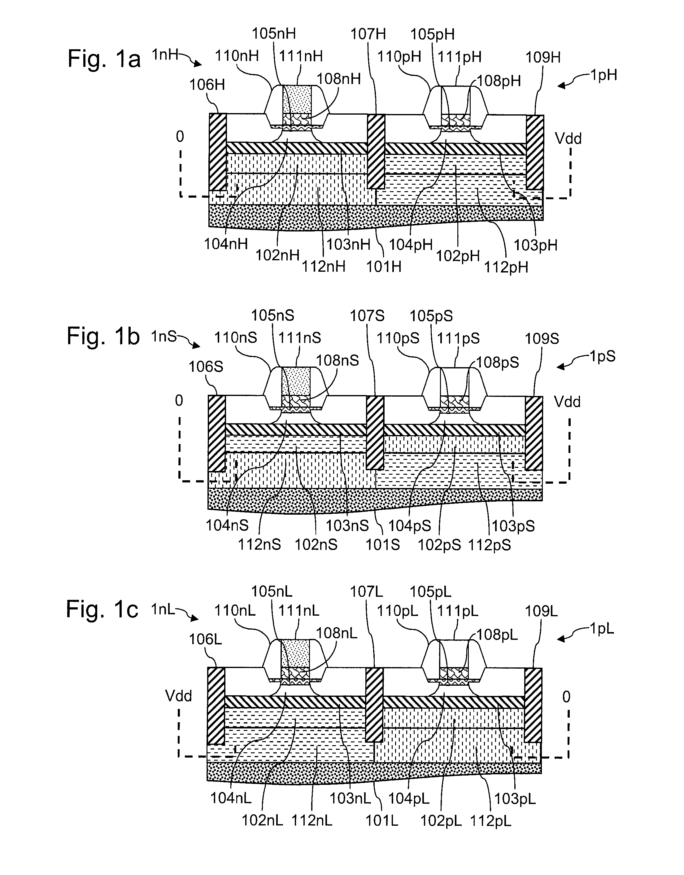
[0046]As illustrated in FIG. 2, a SRAM memory cell consists of two inverters Inv1 and Inv2 connected in a bistable flip-flop configuration and two access transistors MAT and MAF connected to bit lines BLT and BLF. The access transistors MAT and MAF are controlled by a word line WL. The requirements that the memory cell must meet are:[0047]sufficient stability ensuring the operation of the cell during read, write and retention operations;[0048]a maximum conduction current to increase the speed of access to the cell;[0049]a minimum cell size to increase the integration density; and[0050]a minimum retention current to reduce the static electrical consumption.

[0051]FIG. 3 is an electrical diagram of a 6T type memory cell 4 of an integrated circuit according to the invention. The memory cell 4 of FIG. 3 is designed to optimize electrical consumption with improved efficiency and improved functions by reducing causes of dispersions, and enabling simplified dynamic control of the biasing vo...


PUM


Abstract

An integrated circuit on a semiconductor substrate has logic gates comprising FDSOI-type transistors made on said substrate, including at least one first transistor comprising a gate with a first work function, and including a transistor comprising a second work function, a memory including memory cells, each memory cell comprising FDSOI type transistors, including at least one third nMOS transistor with a gate presenting a third work function, the third transistor comprising a buried insulating layer and a ground plane at least one fourth pMOS transistor with a gate presenting said third work function, the fourth transistor comprising a buried insulating layer and a ground plane, the ground planes of the third and fourth transistors being made in a same well separating these ground planes from said substrate.

Description

RELATED APPLICATIONS[0001]Under 35 USC 119, this application claims the benefit of the priority date of French application FR 1,157,997, filed on Sep. 8, 2011, the contents of which are herein incorporated by reference.FIELD OF INVENTION[0002]The invention pertains to integrated circuits and especially to integrated circuits on a silicon-on-insulator (SOI) type substrate. SOI technology consists in separating a thin layer of silicon (a few nanometers thick) from a silicon substrate by a relatively thick (generally a few tens of nanometers) layer of insulator.BACKGROUND[0003]In most advanced integrated circuits, the embedded memory blocks amount to more than half of the total surface area of the circuit. In the future, it is expected that the memory blocks will exceed more than 70% of the total surface area of the circuit. The surface area of the memory cell therefore plays a vital role in the race towards miniaturization. For many years, the gain in integration density has been obta...

Claims


Application Information

Patent Timeline
Patent Type & Authority Applications(United States)
IPC IPC(8): H01L21/336H10B10/00
CPCH01L21/823892H01L21/84H01L27/0928H01L29/78648H01L27/1203H01L27/1052H01L27/1104H10B10/12H10B99/00
Inventor THOMAS, OLIVIERMAZURIER, JEROMEPLANES, NICOLASWEBER, OLIVIER
Owner COMMISSARIAT A LENERGIE ATOMIQUE ET AUX ENERGIES ALTERNATIVES
Features
  • Generate Ideas
  • Intellectual Property
  • Life Sciences
  • Materials
  • Tech Scout
  • Unparalleled Data Quality
  • Higher Quality Content
  • 60% Fewer Hallucinations
Learn More