Interface layer improvements for nonvolatile memory applications

a nonvolatile memory and interface layer technology, applied in the direction of bulk negative resistance effect devices, semiconductor devices, electrical equipment, etc., can solve the problems of difficult to use low resistance metal oxide films to form reliable nonvolatile memory devices, difficult to reduce the operating current of the device, and the resistance of these films and/or the ratio of high-to-low resistance states is often insufficient to be of use within a practical nonvolatile memory device.

Inactive Publication Date: 2013-03-14
KK TOSHIBA +1
View PDF6 Cites 14 Cited by
  • Summary
  • Abstract
  • Description
  • Claims
  • Application Information

AI Technical Summary

Benefits of technology

[0012]Embodiments of the present invention generally provide methods of fabricating a resistive switching nonvolatile memory device having an engineered interface layer disposed between a highly doped silicon electrode and a variable resistance layer in order to reduce the operating current of the device.

Problems solved by technology

However, as device dimensions shrink, scaling issues are posing challenges for traditional nonvolatile memory technology.
Although metal oxide films such as these exhibit bistability, the resistance of these films and / or the ratio of the high-to-low resistance states is (are) often insufficient to be of use within a practical nonvolatile memory device.
Since the variation in the difference between the high and low resistive states is related to the resistance of the resistive switching layer, it is often hard to use a low resistance metal oxide film to form a reliable nonvolatile memory device.
For example, in a nonvolatile memory that has conductive lines fabricated of a relatively high resistance metal such as tungsten, the resistance of the conductive lines may overwhelm the resistance of the metal oxide resistive switching element.
This may make it difficult or impossible to sense the state of the bistable metal oxide resistive switching element.
Similar issues can arise from integration of the resistive switching memory element with current steering elements, such as diodes and / or resistors.
However, since the power that can be delivered to a circuit containing a series of resistive switching memory elements and current steering elements is typically limited in most conventional nonvolatile memory devices (e.g., CMOS driven devices), it is desirable to form each of the resistive switching memory elements and current steering elements in the circuit so that the voltage drop across each of these elements is small, and thus resistance of the series connected elements does not cause the current to decrease to an undesirable level due to the fixed applied voltage (e.g., ˜2-5 volts).

Method used


Image

  • Interface layer improvements for nonvolatile memory applications
  • Interface layer improvements for nonvolatile memory applications
  • Interface layer improvements for nonvolatile memory applications

Examples


Embodiment Construction

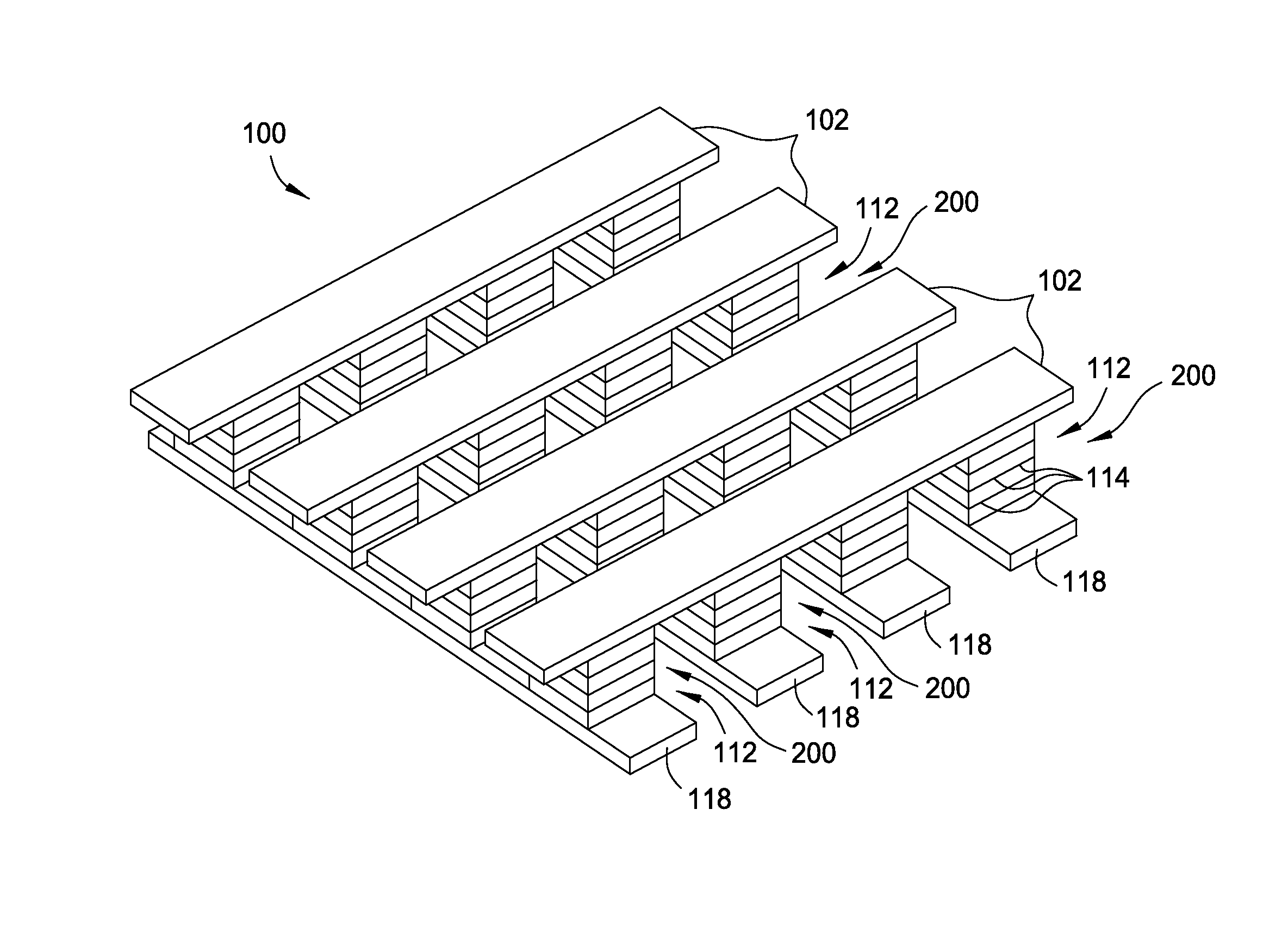
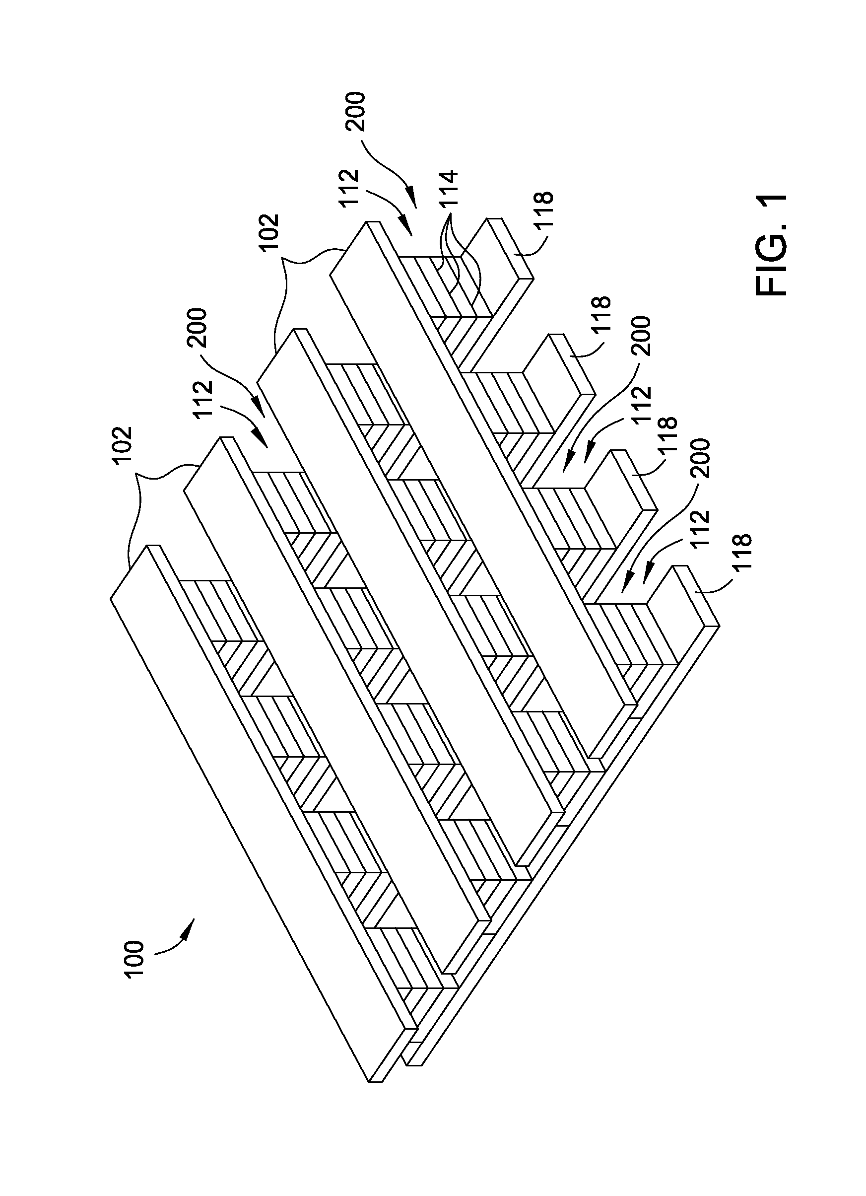
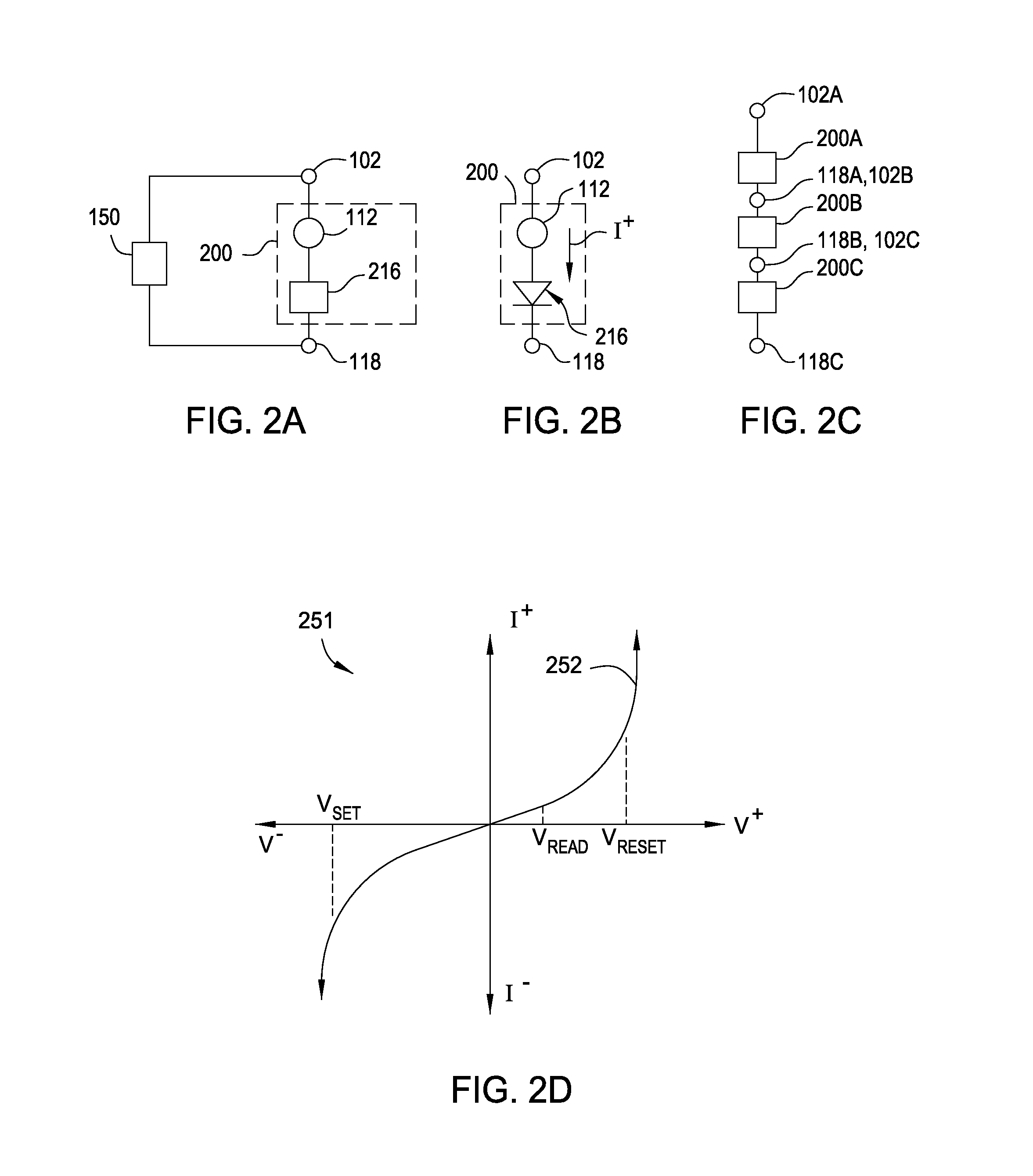
[0027]Embodiments of the invention generally relate to a resistive switching nonvolatile memory device having an interface layer disposed between a highly doped silicon electrode and a variable resistance layer fabricated in the nonvolatile memory device, and methods of fabricating the same. In one embodiment, the interface layer is a high-k layer having a lower electrical effective oxide thickness than native silicon oxide to act as a diffusion barrier between the variable resistance layer and the silicon electrode. The high-k interface layer also increases the barrier height for electron injection / tunneling at the interface between the silicon electrode and the variable resistance layer, which inhibits the flow of current at the interface, reducing switching currents and voltages of the nonvolatile memory device. In another embodiment, the interface layer is a fabricated silicon oxide layer resulting in an improved diffusion barrier between the variable resistance layer and the si...


PUM


Abstract

A resistive switching nonvolatile memory device having an interface layer disposed between a doped silicon electrode and a variable resistance layer fabricated in the nonvolatile memory device and methods of fabricating the same. In one embodiment, the interface layer is a high-k layer having a lower electrical EOT than native silicon oxide to act as a diffusion barrier between the variable resistance layer and the silicon electrode. Alternatively, the high-k interface layer may be formed by performing a nitrogen treatment on a fabricated silicon oxide layer. In another embodiment, the interface layer may be fabricated by performing a nitrogen or ozone treatment on the native oxide layer. In another embodiment, the interface layer is a fabricated silicon oxide layer resulting in an improved diffusion barrier between the variable resistance layer and the silicon electrode. In all embodiments, the interface layer also passivates the surface of the silicon electrode.

Description

BACKGROUND OF THE INVENTION[0001]1. Field of the Invention[0002]wan This invention relates to nonvolatile memory elements, and more particularly, to methods for forming resistive switching memory elements used in nonvolatile memory devices.[0003]2. Description of the Related Art[0004]Nonvolatile memory elements are used in systems in which persistent storage is required. For example, digital cameras use nonvolatile memory cards to store images and digital music players use nonvolatile memory to store audio data. Nonvolatile memory is also used to persistently store data in computer environments.[0005]Nonvolatile memory is often fabricated using electrically-erasable programmable read only memory (EPROM) technology. This type of nonvolatile memory contains floating gate transistors that can be selectively programmed or erased by application of suitable voltages to their terminals.[0006]As fabrication techniques improve, it is becoming possible to fabricate nonvolatile memory elements...

Claims


Application Information

Patent Timeline
Patent Type & Authority Applications(United States)
IPC IPC(8): H01L47/00
CPCH01L45/04H01L45/1233H01L27/2463H01L27/2409H01L45/146H10B63/20H10B63/80H10N70/24H10N70/801H10N70/023H10N70/041H10N70/826H10N70/8833
Inventor GOPAL, VIDYUTWANG, YUNHASHIM, IMRAN
Owner KK TOSHIBA
Why Eureka
Try Eureka