Semiconductor device

a technology of semiconductors and semiconductors, applied in the direction of semiconductor devices, basic electric elements, electrical equipment, etc., can solve the problems of reduced wiring of transistors, high contact resistance, and miniaturization-induced defects, and achieve high contact resistance and favorable electrical characteristics. , the effect of high reliability

Inactive Publication Date: 2013-03-21
SEMICON ENERGY LAB CO LTD
View PDF4 Cites 37 Cited by
  • Summary
  • Abstract
  • Description
  • Claims
  • Application Information

AI Technical Summary

Benefits of technology

[0032]One embodiment of the present invention can provide a semiconductor device which has favorable electrical characteristics and is miniaturized. One embodiment of the present invention can provide a highly reliable semiconductor device. One embodiment of the present invention can provide a method for manufacturing the semiconductor device.

Problems solved by technology

However, defects are caused by the miniaturization.
For example, when a transistor is miniaturized, the area of contact between a semiconductor layer and a wiring of the transistor is reduced, and thus, a problem such as high contact resistance occurs.
High contact resistance leads to degradation in electrical characteristics such as a small on-state current of the transistor.

Method used


Image

  • Semiconductor device
  • Semiconductor device
  • Semiconductor device

Examples


embodiment 1

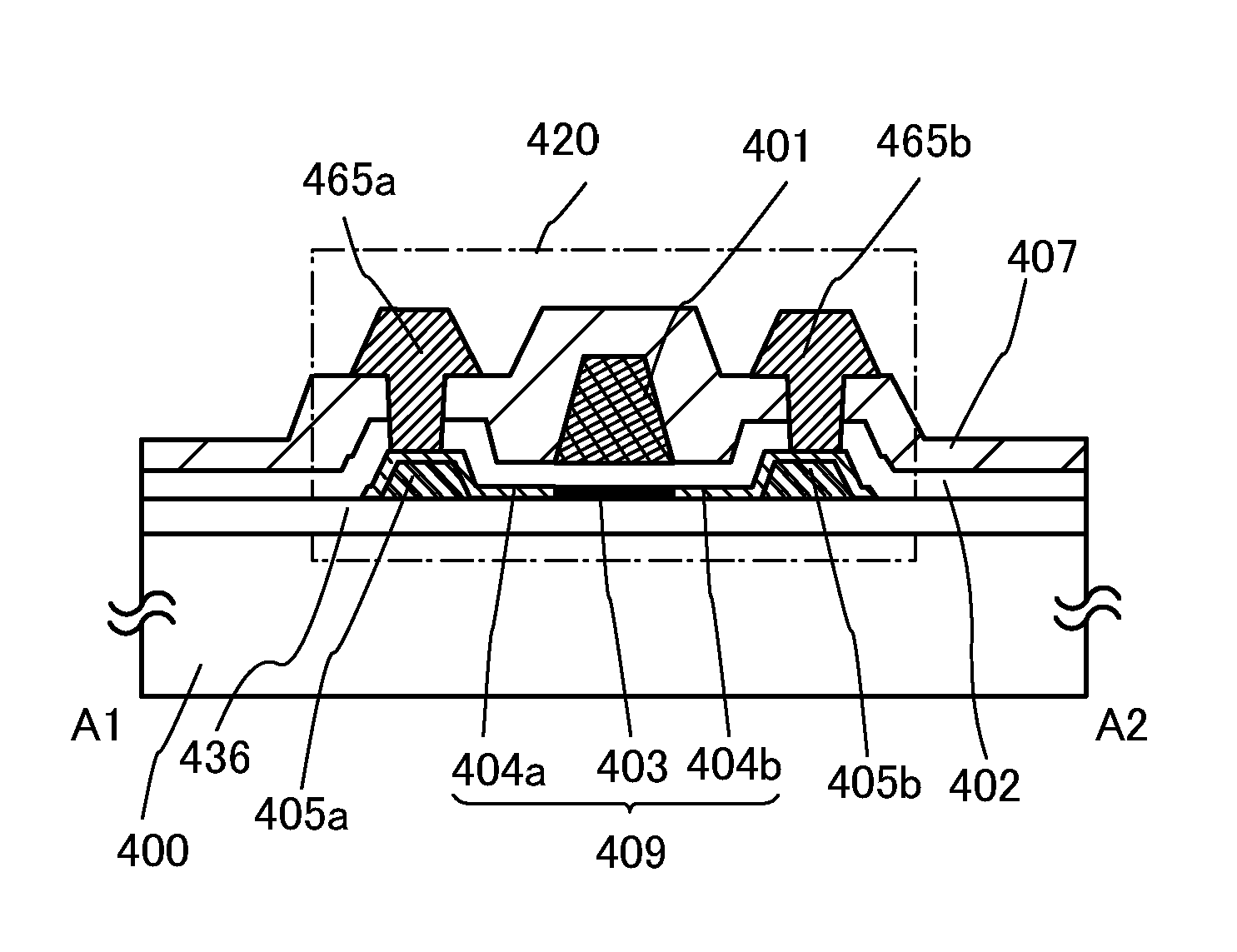
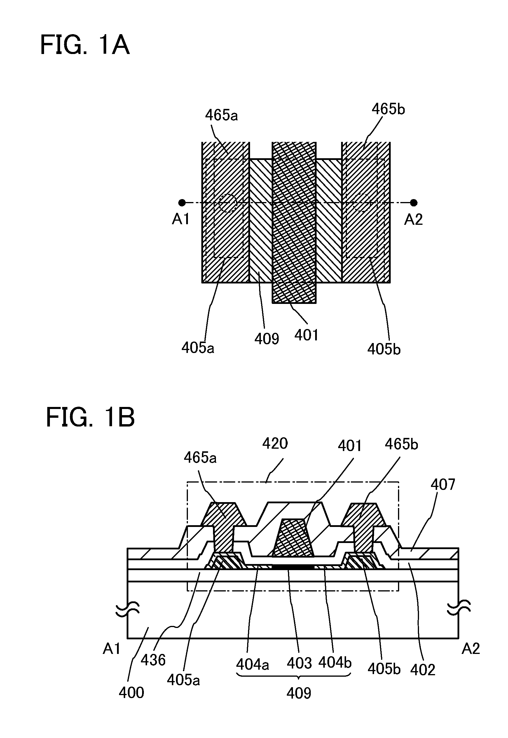
[0055]In this embodiment, a basic structure and a basic manufacturing method of a semiconductor device of one embodiment of the present invention are described with reference to drawings. FIGS. 1A and 1B illustrate a semiconductor device of one embodiment of the present invention. FIG. 1A is a top view of a transistor which is one embodiment of the present invention, and FIG. 1B is a cross-sectional view taken along dashed-dotted line A1-A2 in FIG. 1A.

[0056]A transistor 420 shown in FIGS. 1A and 1B includes a base insulating layer 436 over a substrate 400; an electrode layer 405a and an electrode layer 405b over the base insulating layer 436; an oxide semiconductor layer 409 over the base insulating layer 436, the electrode layer 405a, and the electrode layer 405b; a gate insulating layer 402 covering the oxide semiconductor layer 409; a gate electrode layer 401 over the gate insulating layer 402; an insulating layer 407 over the gate insulating layer 402 and the gate electrode laye...

embodiment 2

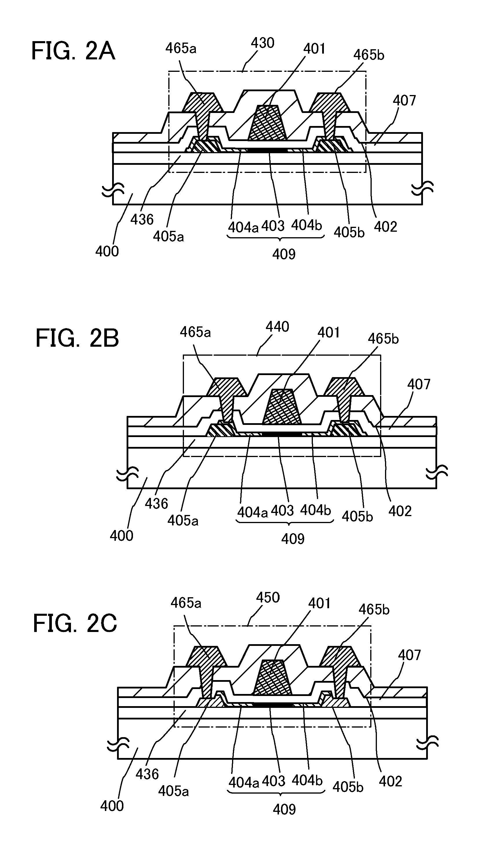
[0158]In this embodiment, semiconductor devices of embodiments which are different from those of the semiconductor devices described in Embodiment 1 are described. Note that, in this embodiment, portions that are similar to the portions in Embodiment 1 are denoted by the same reference numerals, and detailed description thereof is omitted.

[0159]FIGS. 15A and 15B illustrate a transistor of one embodiment of the present invention. FIG. 15A is a top view illustrating a semiconductor device of one embodiment of the present invention, and FIG. 15B is a cross-sectional view taken along dashed-dotted line A3-A4 in FIG. 15A.

[0160]A transistor 1420 shown in FIGS. 15A and 15B includes a base insulating layer 436 over a substrate 400; an electrode layer 405a and an electrode layer 405b over the base insulating layer 436; an oxide semiconductor layer 409 over the base insulating layer 436, the electrode layer 405a, and the electrode layer 405b; a gate insulating layer 402 covering the oxide sem...

embodiment 3

[0193]In this embodiment, an example of a semiconductor device which includes the transistor described in Embodiments 1 and 2, which can hold stored data even when not powered, and which does not have a limitation on the number of write cycles, will be described with reference to drawings. Note that a transistor 162 included in the semiconductor device in this embodiment is the transistor described in Embodiment 1. Any of the transistors described in Embodiments 1 and 2 can be used as the transistor 162.

[0194]Since the off-state current of the transistor 162 is small, stored data can be held for a long time owing to such a transistor. In other words, power consumption can be sufficiently reduced because a semiconductor memory device in which refresh operation is unnecessary or the frequency of refresh operation is extremely low can be provided.

[0195]FIGS. 8A to 8C illustrate an example of a structure of a semiconductor device. FIG. 8A is a cross-sectional view of the semiconductor d...


PUM


Abstract

Provided is a semiconductor device in which an oxide semiconductor layer is provided; a pair of wiring layers which are provided with the gate electrode layer interposed therebetween are electrically connected to the low-resistance regions; and electrode layers are provided to be in contact with the low-resistance regions, below regions where the wiring layers are formed.

Description

BACKGROUND OF THE INVENTION[0001]1. Field of the Invention[0002]One embodiment of the present invention relates to a semiconductor device and a method for manufacturing the semiconductor device.[0003]2. Description of the Related Art[0004]Attention has been focused on a technique for forming a transistor (also referred to as a thin film transistor (TFT)) using a thin semiconductor film formed over a substrate having an insulating surface.[0005]For example, a transistor whose active layer includes an amorphous oxide including indium (In), gallium (Ga), and zinc (Zn) is disclosed (see Patent Document 1).REFERENCEPatent Document[0006][Patent Document 1] Japanese Published Patent Application No. 2006-165528SUMMARY OF THE INVENTION[0007]Also in the case of a transistor including an oxide semiconductor, it is important to miniaturize the transistor in order to achieve high-speed operation, low power consumption, cost reduction, or the like of the transistor.[0008]However, defects are caus...

Claims


Application Information

Patent Timeline
Patent Type & Authority Applications(United States)
IPC IPC(8): H01L29/78
CPCH01L29/41733H01L29/78693H01L29/7869H01L29/78618H01L27/1225H01L27/124H01L29/45
Inventor YAMAZAKI, SHUNPEIISOBE, ATSUOGODO, HIROMACHIHATANO, TAKEHISATEZUKA, SACHIAKIHONDO, SUGURUYAMADE, NAOTOKOEZUKA, JUNICHI
Owner SEMICON ENERGY LAB CO LTD
Why Eureka
Try Eureka