Mask blank glass substrate, multilayer reflective film coated substrate, mask blank, mask, and methods of manufacturing the same

a reflective film and mask technology, applied in the field of masks, can solve the problems of difficult to achieve high smoothness, difficult to reuse or recycle substrates by stripping, and often used high-value-added expensive substrates, and achieve the effect of enhancing the detection accuracy of a defect position

Active Publication Date: 2013-03-28
HOYA CORP
View PDF1 Cites 36 Cited by
  • Summary
  • Abstract
  • Description
  • Claims
  • Application Information

AI Technical Summary

Benefits of technology

[0081]According to this invention, it is possible to provide a mask blank glass substrate and a multilayer reflective film coated substrate having a multilayer reflective film on the mask blank glass substrate that can each suppress false defect detection in a highly sensitive defect inspection apparatus to thereby enhance the detection accuracy of a defect position or the like using a fiducial mark as a reference and that each enable recycling of a glass substrate included therein, and further to provide methods of manufacturing them.
[0082]Furt

Problems solved by technology

However, according to such a conventional method, a fiducial mark is formed by digging down a substrate (generally a glass substrate) for a mask blank and, therefore, for example, in the case of a mask blank whose surface defect is found after forming a pattern-formation thin film on the substrate or in the case of a transfer mask which is produced using a mask blank and in which a pattern defect that is difficult to correct is found, it is difficult to reuse or recycle the substrate by stripping and removing the thin film from the substrate without discarding the mask blank or the transfer mask as a defective.
Further, in recent years, with the miniaturization of patterns in semiconductor devi

Method used


Image

  • Mask blank glass substrate, multilayer reflective film coated substrate, mask blank, mask, and methods of manufacturing the same
  • Mask blank glass substrate, multilayer reflective film coated substrate, mask blank, mask, and methods of manufacturing the same
  • Mask blank glass substrate, multilayer reflective film coated substrate, mask blank, mask, and methods of manufacturing the same

Examples


example 1

[0199]1)>

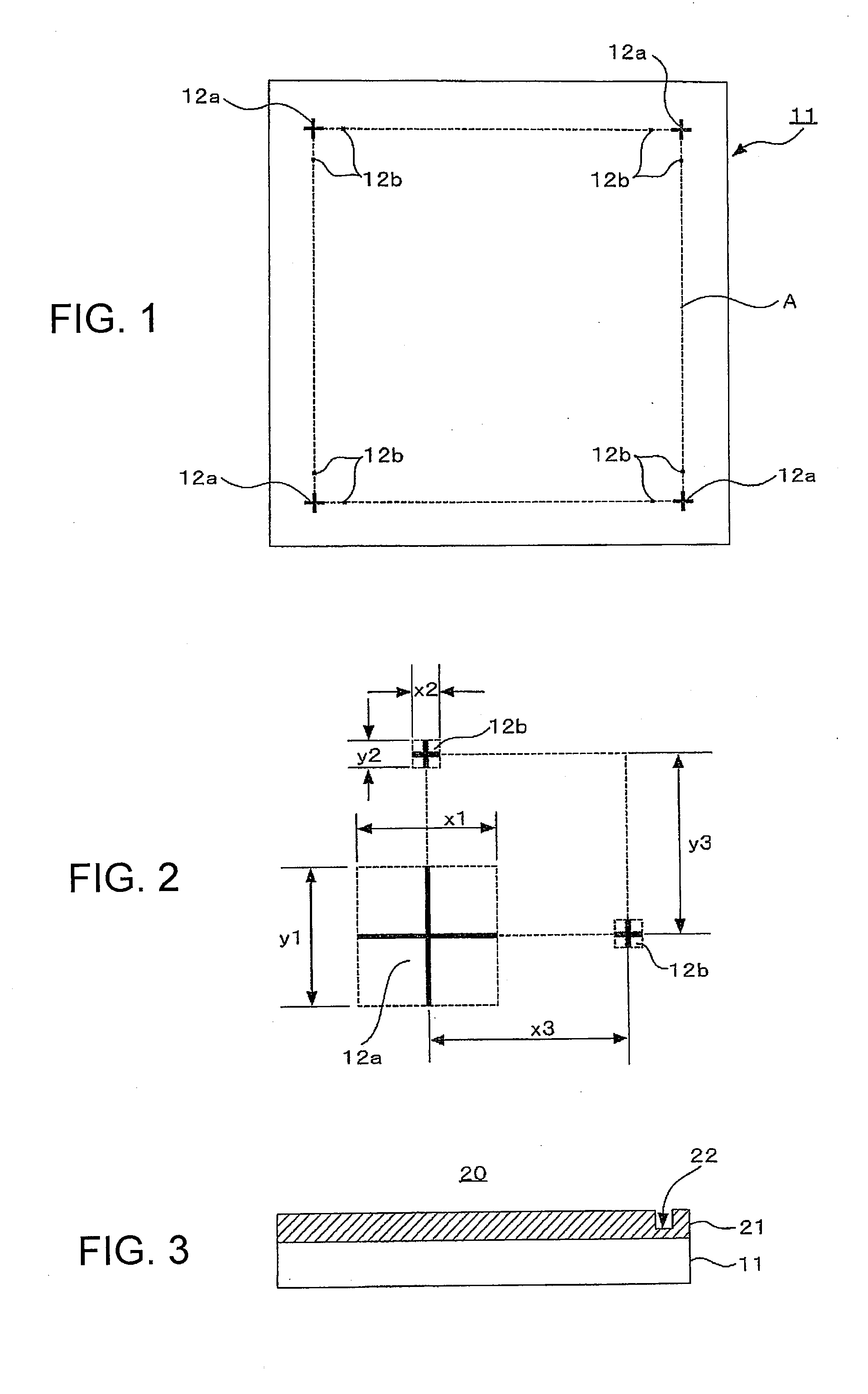
[0200]A SiO2-TiO2-based glass substrate (size: about 152.4 mm×about 152.4 mm, thickness: about 6.35 mm) was prepared. Specifically, using a double-side polishing machine, both front and back surfaces of the glass substrate were polished stepwise with cerium oxide abrasive particles and colloidal silica abrasive particles and then treated with low-concentration fluorosilicic acid. The surface roughness of the prepared glass substrate, measured by AFM (atomic force microscope), was 0.25 nm in RMS (measurement region: 1 μm×1 μm).

[0201]The surface shape (flatness) of both front and back surfaces of the glass substrate was measured by a flatness measuring apparatus (UltraFlat: manufactured by Tropel Corporation) (measurement region: 148 mm×148 mm).

[0202]As a result, the flatness of the front and back surfaces of the glass substrate was about 290 nm.

[0203]The surface shape (flatness) measurement results of the front and back surfaces of the glass substrate were each stored in a c...

example 2

[0240]In Example 1, a CrN underlayer (Cr: 90 at %, N: 10 at %) having an amorphous crystal structure was used instead of the Si underlayer. Specifically, using a Cr target and using a mixed gas of Ar, He, and N2 as a sputtering gas, DC magnetron sputtering was carried out to form a CrN underlayer having a thickness of 100 nm.

[0241]A surface of the CrN underlayer was precision-polished in the same manner as in Example 1. As a result, in a 142 mm×142 mm measurement region, the flatness was 85 nm and thus satisfied the target value of 100 nm or less. Further, in a 1 μm ×1 μm measurement region, the surface roughness was 0.10 nm in RMS and thus was satisfactory.

[0242]Since the surface of the CrN underlayer has an extremely high smoothness of 0.1 nm or less in RMS, background noise in a highly sensitive defect inspection apparatus is reduced, which is effective in terms of suppressing false defect detection.

[0243]Further, in a 1 μm ×1 μm measurement region, the maximum surface roughness ...

example 3

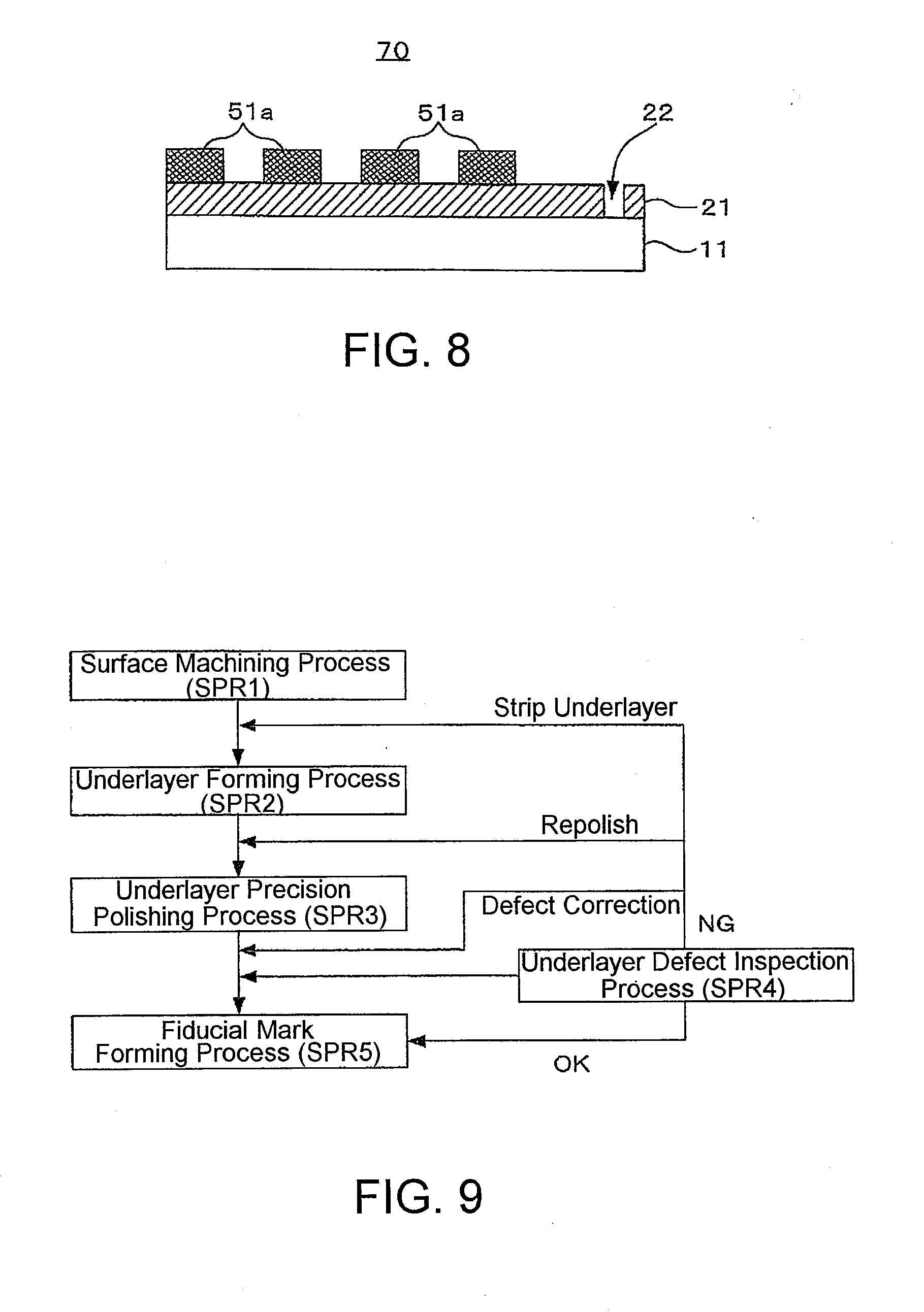
[0251]Next, a description will be given of an example where, in Example 2, defects are found in the defect inspection of the underlayer so that the underlayer is stripped to recycle the glass substrate.

[0252]Since a number of defects having a size of 60 nm were detected in the defect inspection of the surface of the CrN underlayer using the mask blank defect inspection apparatus (MAGICS M1350: manufactured by Lasertec Corporation) (inspection region: 142 mm×142 mm), the CrN underlayer was entirely dry-etched with a mixed gas of Cl2 and 02 to be removed.

[0253]In this case, the SiO2-TiO2-based glass is not etched with the mixed gas of Cl2 and O2. Therefore, the surface roughness of the main surface of the glass substrate after stripping the CrN underlayer was measured to be 0.4 nm in RMS. The flatness was 80 nm and thus was satisfactory.

[0254]After stripping the CrN underlayer, the glass substrate was cleaned with an alkaline aqueous solution and then a CrN underlayer was formed again...


PUM


Abstract

Provided is a mask blank glass substrate that has high surface smoothness, that is formed with a fiducial mark capable of improving the detection accuracy of a defect position or the like, and that enables reuse or recycling of a glass substrate included therein. An underlayer is formed on a main surface, on the side where a transfer pattern is to be formed, of a glass substrate for a mask blank. The underlayer serves to reduce surface roughness of the main surface of the glass substrate or to reduce defects of the main surface of the glass substrate. A surface of the underlayer is a precision-polished surface. A fiducial mark which provides a reference for a defect position in defect information is formed on the underlayer.

Description

[0001]This application is based upon and claims the benefit of priority from Japanese patent application No. 2011-212207, filed on Sep. 28, 2011, and Japanese patent application No. 2012-170911, filed on Aug. 1, 2012, the disclosures of which are incorporated herein in their entirety by reference.TECHNICAL FIELD[0002]This invention relates to a mask blank glass substrate, a multilayer reflective film coated substrate, a mask blank, and a mask which are adapted for use in the manufacture of semiconductor devices or the like, and further relates to methods of manufacturing the same.BACKGROUND ART[0003]Generally, fine pattern formation is carried out by the photolithography in the manufacture of a semiconductor device. A number of transfer masks called photomasks are normally used for such fine pattern formation. The transfer mask comprises generally a transparent glass substrate having thereon a fine pattern made of a metal thin film or the like. The photolithography is used also in t...

Claims


Application Information

Patent Timeline
IPC IPC(8): G03F1/24
CPCG03F1/24G03F1/60G03F1/38G03F1/76H01L21/0274
Inventor ORIHARA, TOSHIHIKOKAWAHARA, AKIHIROSHOKI, TSUTOMU
Owner HOYA CORP
Why Eureka
Try Eureka