Method for depositing a gate oxide and a gate electrode selectively

Inactive Publication Date: 2013-03-28
FUDAN UNIV
View PDF9 Cites 36 Cited by
  • Summary
  • Abstract
  • Description
  • Claims
  • Application Information

AI Technical Summary

Benefits of technology

[0008]In view of this, the present invention aims at providing a method for manufacturing a gate through selective deposition technology to r

Problems solved by technology

With the continuous reduction of the feature size of Metal-Oxide-Semiconductor Field Effect Transistors (MOSFET), the insulated gate dielectric layer is also becoming thinner and thinner according to the principle of reducing in equal proportion, and when the gate dielectric layer is thin enough, problems such as its reliability, especially the time-related breakdown and the impurities in gate electrodes diffusing into the substrate will seriously influence the stability and reliability of devices.
Now, SiO2 as the gate dielectric has reached its physical limit, and the quantum direct tunneling effect will lead to a remarkable increase of leakage curr

Method used


Image

  • Method for depositing a gate oxide and a gate electrode selectively
  • Method for depositing a gate oxide and a gate electrode selectively
  • Method for depositing a gate oxide and a gate electrode selectively

Examples


Embodiment Construction

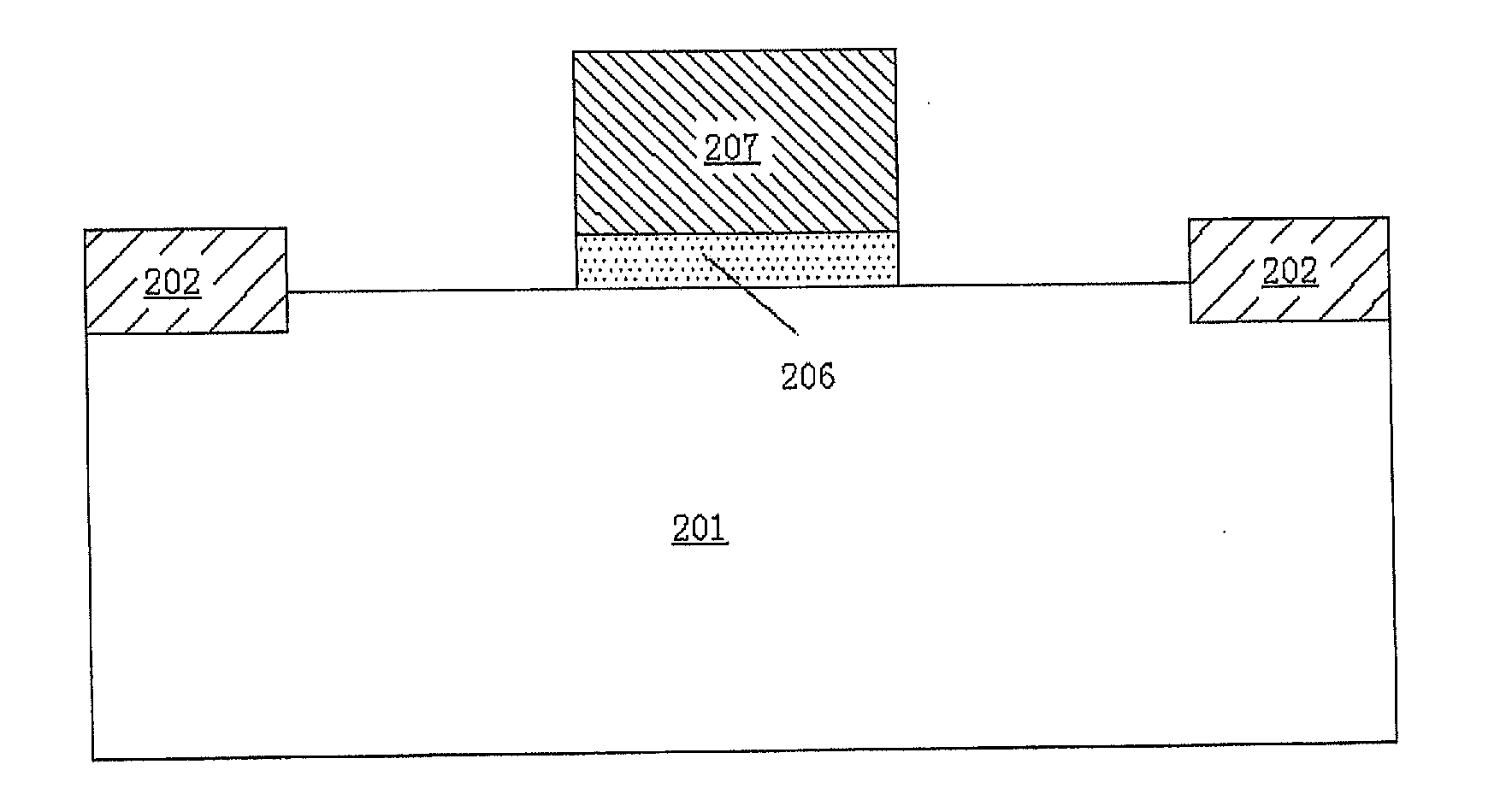
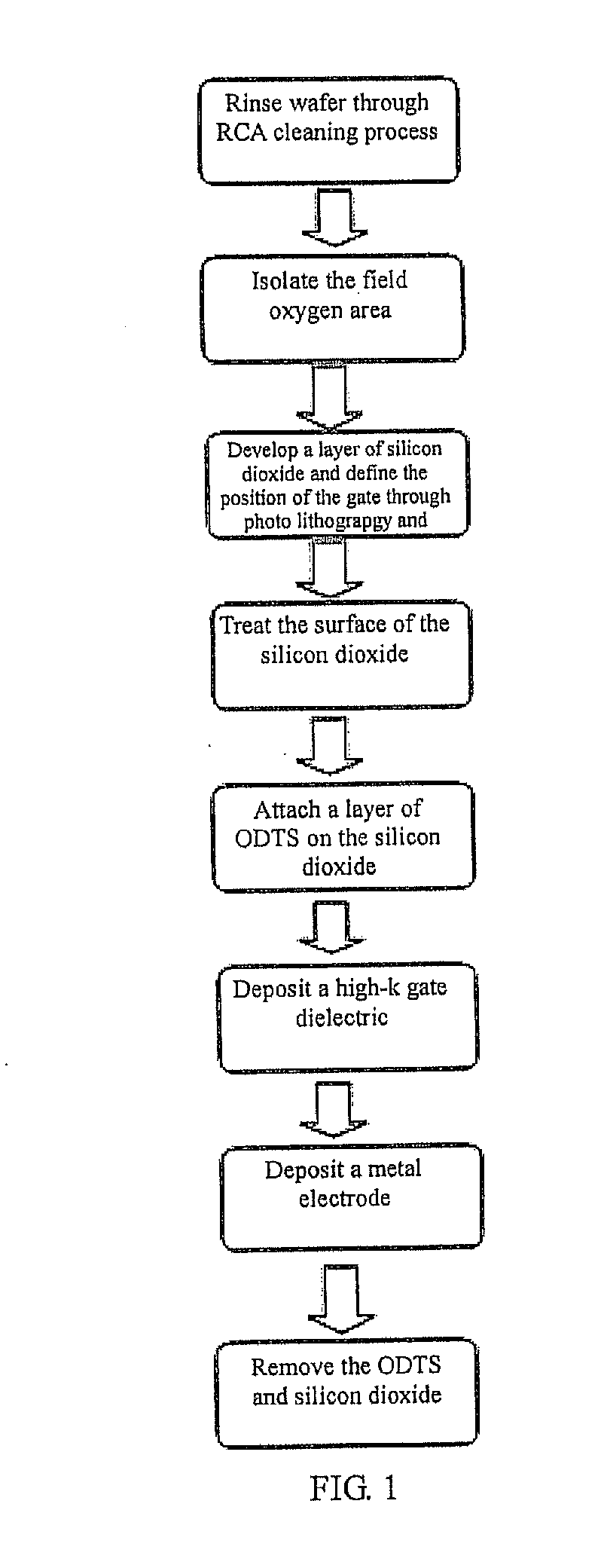
[0029]FIG. 1 is a process flow diagram of the method for depositing a gate oxide and a gate electrode selectively provided by the present invention. The method includes the following steps: provide a semiconductor substrate and rinse it through the RCA cleaning process; isolate the field oxide area; develop a layer of silicon dioxide; define the position of the gate through photo lithography and etching; treat the surface of the silicon dioxide; attach a layer of ODTS on the silicon dioxide; deposit a high-k gate dielectric; deposit a metal electrode; remove the ODTS and silicon dioxide.

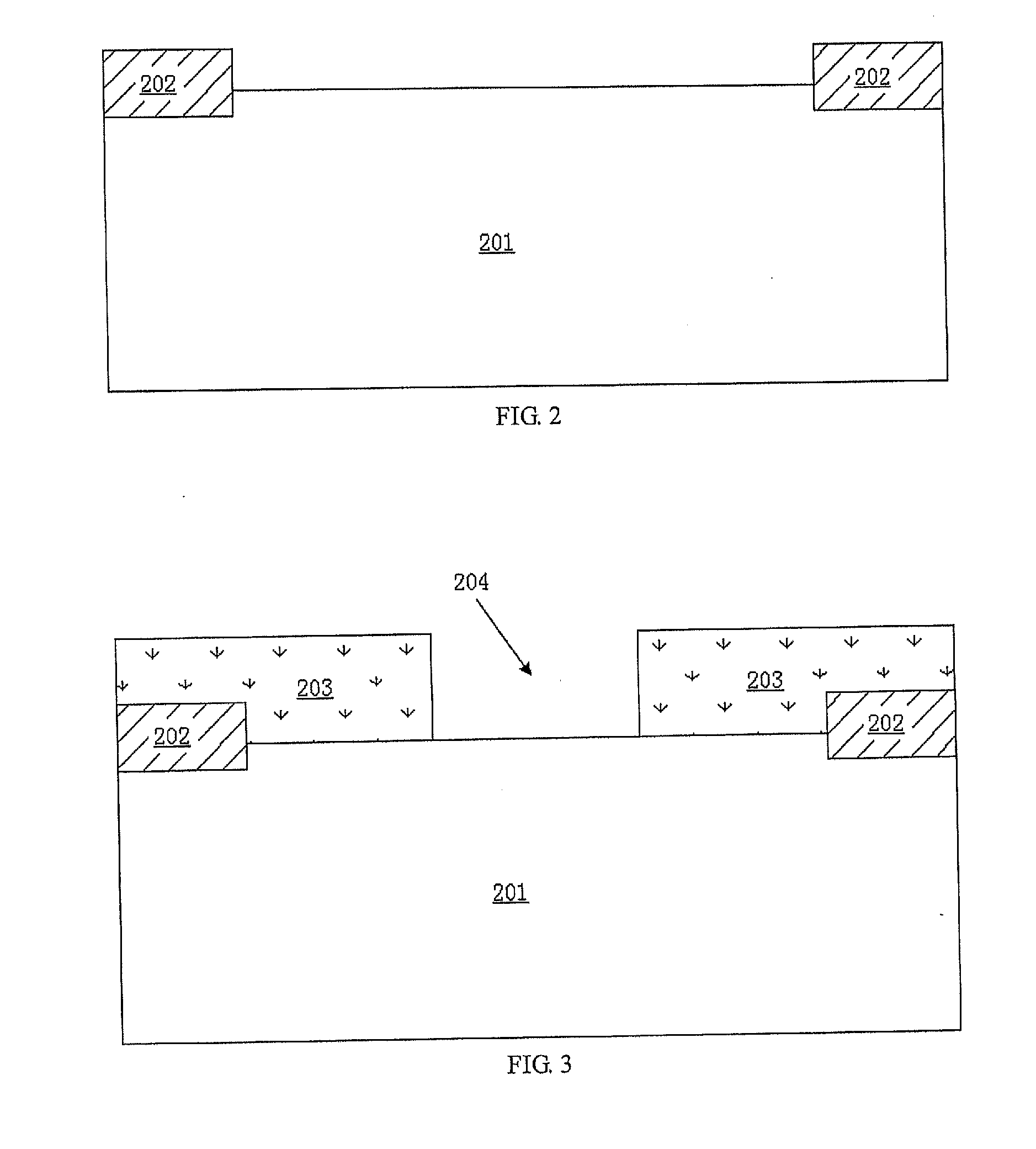
[0030]The present invention is further detailed in combination with the drawings and the embodiments below. In the drawings, the thicknesses of layers and regions are either zoomed in or out for the convenience of description, so it shall not be considered as the true size. Although the drawings cannot accurately reflect the true size of the devices, they still reflect the relative position among reg...


PUM


Abstract

The present invention belongs to the technical field of integrated semiconductor circuits, and relates to a method for depositing a gate oxide and a gate electrode selectively. The present invention makes use of Octadecyltriethoxysilane's (ODTS') easy attachment to the Si—OH interface and difficult attachment to the Si—H interface, and selectively deposits the gate oxide and gate electrode materials, which avoids the unnecessary waste of materials and saves cost. Meanwhile, the present invention will transfer the etching of the gate oxide and gate electrode into the etching of SiO2 so as to reduce the difficulty of the etching process and increase the production efficiency.

Description

CROSS-REFERENCE TO RELATED APPLICATION[0001]This application is a continuation of and claims priority to Chinese Patent Application No. CN201110285019.1 filed on Sep. 23, 2011, the entire content of which is incorporated by reference herein.BACKGROUND OF THE INVENTION[0002]1. Technical Field[0003]The present invention belongs to the technical field of integrated semiconductor circuit, relates to a method for manufacturing a gate oxide and a gate electrode, and more specifically, to a method for depositing a gate oxide and a gate electrode selectively.[0004]2. Description of Related Art[0005]With the continuous reduction of the feature size of Metal-Oxide-Semiconductor Field Effect Transistors (MOSFET), the insulated gate dielectric layer is also becoming thinner and thinner according to the principle of reducing in equal proportion, and when the gate dielectric layer is thin enough, problems such as its reliability, especially the time-related breakdown and the impurities in gate el...

Claims


Application Information

Patent Timeline
IPC IPC(8): H01L21/28
CPCH01L21/28194H01L29/517H01L29/495H01L29/4966H01L21/02307H01L21/02164H01L21/02178H01L21/02181H01L29/66583
Inventor SUN, QINGQINGLI, YEFANG, RUNCHENWANG, PENGFELZHANG, WEI
Owner FUDAN UNIV
Why Eureka
Try Eureka