Semiconductor device and fabrication method thereof

a semiconductor device and semiconductor technology, applied in semiconductor devices, diodes, electrical devices, etc., can solve the problems of reducing the length of the gate, affecting and affecting the thickness of the gate oxide, so as to achieve the effect of improving the performance of the semiconductor devi

Active Publication Date: 2013-04-11
UNITED MICROELECTRONICS CORP
View PDF3 Cites 21 Cited by
  • Summary
  • Abstract
  • Description
  • Claims
  • Application Information

AI Technical Summary

Benefits of technology

[0018]By performing these two separate etching processes respectively thinning the poly-silicon element layer and removing the poly-silicon gate electrode, the passive device and the metal gate can get a coplanar surface on which metal contacts can be formed without remaining undesired metal residues. Therefore the performance of the semiconductor device can be improved significantly.

Problems solved by technology

As each technology nodes shrink, the dimensions of a FET and the thickness of its gate oxide, however, must be reduced and gate leakage could be more likely triggered by the reduced gate length.
However, removing the dummy gate and depositing the metal layer may conversely affect the integration of the metal gate transistor with other semiconductor devices.
Accordingly, device performance may deteriorate.

Method used


Image

  • Semiconductor device and fabrication method thereof
  • Semiconductor device and fabrication method thereof
  • Semiconductor device and fabrication method thereof

Examples


Embodiment Construction

[0022]The present invention is to provide an advanced semiconductor device and the fabricating method thereof used to integrate a metal gate transistor with a passive device. The present invention will now be described more specifically with reference to the following embodiments. It is to be noted that the following descriptions of preferred embodiments of this invention are presented herein for purpose of illustration and description only. It is not intended to be exhaustive or to be limited to the precise form disclosed.

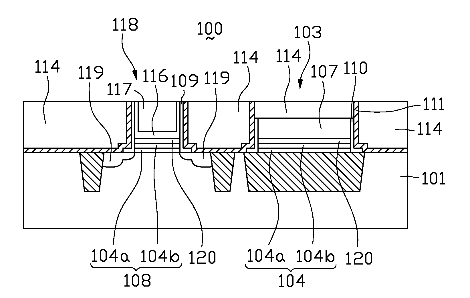
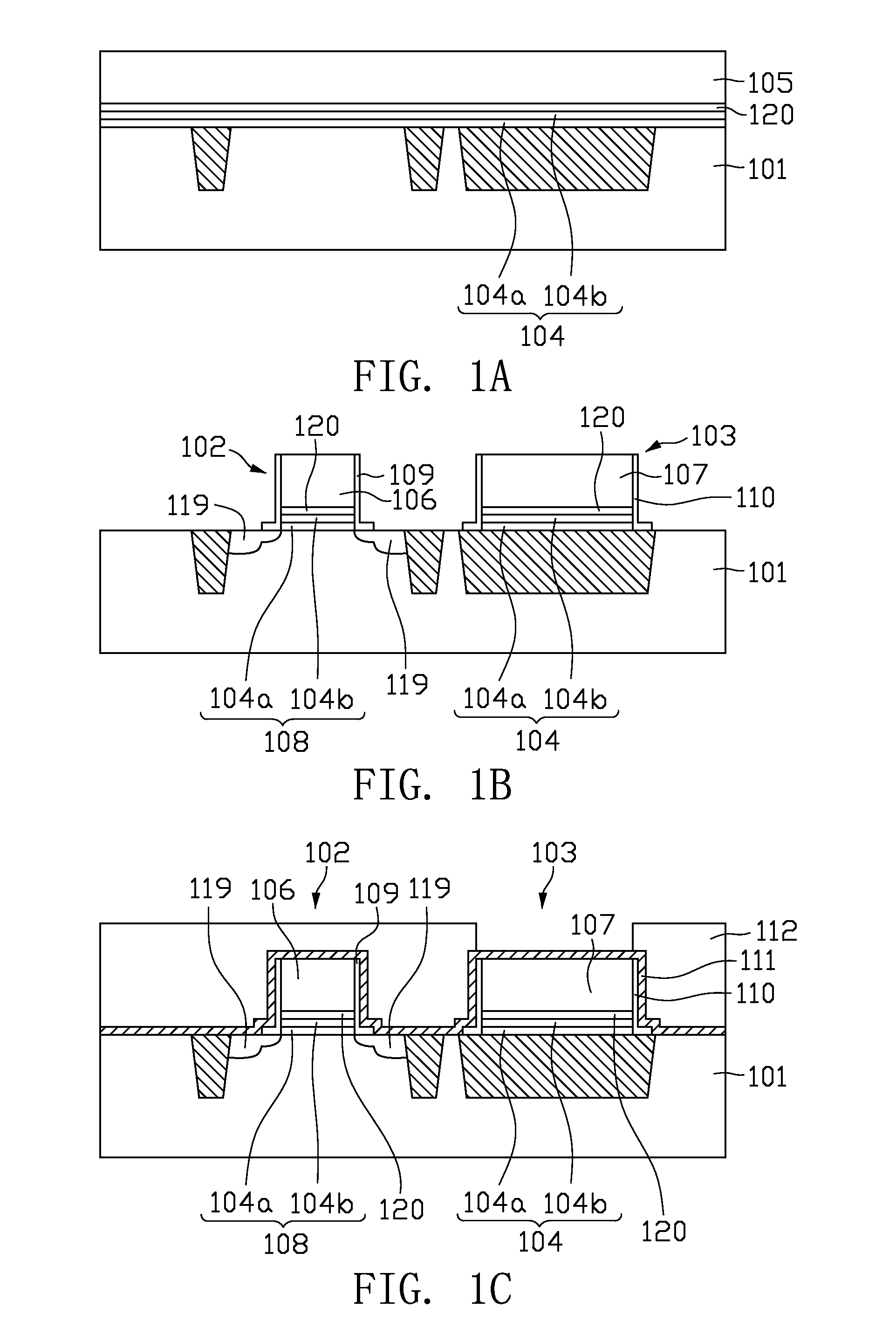
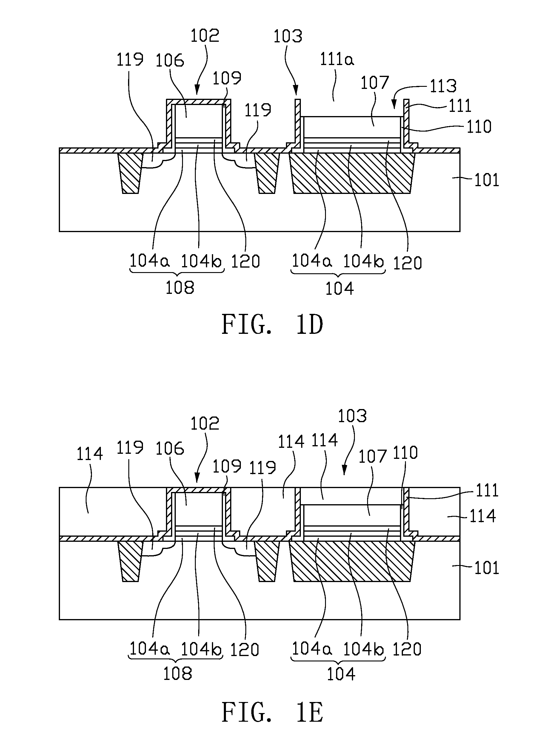
[0023]FIGS. 1A to 1G are cross-sectional views illustrating the method for fabricating a semiconductor device 100 in accordance with one embodiment of the present invention, wherein the method comprises steps as follows:

[0024]A substrate 101 having a dielectric material layer 104, a capping layer 120 and a poly-silicon layer 105 sequentially stacked on the substrate 101 is provided (see FIG. 1A). In the present embodiment, the dielectric material layer 104 compris...


PUM

PropertyMeasurementUnit
distanceaaaaaaaaaa
thicknessaaaaaaaaaa
dielectric constantaaaaaaaaaa

Abstract

A semiconductor device comprises a metal gate electrode, a passive device and a hard mask layer. The passive device has a poly-silicon element layer. The hard mask layer is disposed on the metal gate electrode and the passive electrode and has a first opening and a second opening substantially coplanar with each other, wherein the metal gate electrode and the poly-silicon element layer are respectively exposed via the first opening and the second opening; and there is a distance between the first opening and the metal gate electrode substantially less than the distance between the second opening and the poly-silicon element layer.

Description

FIELD OF THE INVENTION[0001]The present invention relates to a semiconductor device and the fabricating method thereof, more particularly to a field effect transistor (FET) with a metal gate and the fabricating method thereof.BACKGROUND OF THE INVENTION[0002]With the development of the electrical technology, a FET with high integrity and operation speed is required. As each technology nodes shrink, the dimensions of a FET and the thickness of its gate oxide, however, must be reduced and gate leakage could be more likely triggered by the reduced gate length.[0003]In order to reduce gate leakage, high dielectric constant (high-k) gate insulator layers are used and the conventional polysilicon gate electrode is replaced with a metal gate (MG) electrode to improve the device performance as the feature sizes has being decreased.[0004]The conventional technique for fabricating a metal gate transistor includes the following steps: Firstly a metal-oxide-semiconductor (MOS) transistor with a...

Claims


Application Information

Patent Timeline
Patent Type & Authority Applications(United States)
IPC IPC(8): H01L27/10H01L21/8234
CPCH01L27/0629H01L21/027H01L21/8232H01L21/3212H01L21/32139H01L21/28079
Inventor CHEN, CHIEH-TETZOU, SHIH-FANGLIAO, JIUNN-HSIUNGLIN, YI-PO
Owner UNITED MICROELECTRONICS CORP
Why Eureka
Try Eureka