Method for manufacturing bonded wafer

a technology of bonded wafers and bonded layers, which is applied in the direction of semiconductor/solid-state device manufacturing, basic electric elements, electric apparatus, etc., can solve the problems of reducing the dopant concentration of the soi layer surface, the radial distribution of the soi film thickness of the cmp process deteriorates, and the desired electrical resistivity cannot be maintained, so as to achieve low resistivity, improve the film thickness distribution, and reduce the effect of oxidation

Inactive Publication Date: 2013-04-25
SHIN-ETSU HANDOTAI CO LTD
View PDF4 Cites 9 Cited by
  • Summary
  • Abstract
  • Description
  • Claims
  • Application Information

AI Technical Summary

Benefits of technology

[0023]When the epitaxial layer is formed, for example, on the surface of a p+SOI layer of the SOI wafer subjected to processes up to a flattening heat treatment (gas etching with HCl) to manufacture an SOI wafer having a p− / p+ structure, the manufactured SOI wafer has both a desired structure and an SOI layer with improved film thickness distribution.
[0024]As described above, the present invention can provide a method for manufacturing a bonded wafer having a low resistivity thin film (SOI layer) that contains dopant such as boron with high concentration, in which outward diffusion of dopant and the suction due to oxidation can be inhibited to maintain low resistivity. The method also enables efficient manufacture of a bonded wafer with a thin film (SOI layer) having normal resistivity by utilizing delamination at a low resistivity layer that contains dopant such as boron with high concentration while the resistivity of the normal resistivity layer can be avoided from varying. In addition, according to the present invention, a bonded wafer having improved surface roughness and an SOI layer with good film thickness distribution can be manufactured.

Problems solved by technology

In a method for manufacturing bonded wafers by the ion implantation delamination method, surface roughness after delamination is insufficient and a damaged layer due to ion implantation remains on a surface after delamination; therefore it is necessary to improve the surface roughness and remove the damaged layer.
The CMP process deteriorates a radial distribution of the SOI film thickness due to stock removal distribution of CMP and damages an SOI surface due to CMP.
It is therefore inevitable that the dopant concentration of the SOI layer surface decreases and a desired electrical resistivity cannot be maintained.
When dopant is p-type such as boron, since a suction effect due to segregation of boron into an oxide film is observed in a sacrificial oxidation process for removing the damaged layer, a desired electrical resistivity of the SOI layer cannot be similarly maintained.
In this method, however, a long heat treatment is needed for outward diffusion of boron (See Patent Documents 3 and 4).

Method used


Image

  • Method for manufacturing bonded wafer
  • Method for manufacturing bonded wafer

Examples


example 1 (

Example 1(a), Example 1(b), and Comparative Example

[0057]Three SOI wafers in Table 2 described below among the SOI wafers after the delamination manufactured in the above Experiment were thinned by gas etching with HCl. The surface roughness (RMS and R-V) of each wafer is given in Table 2.

[0058]When the low resistivity wafer was used as the bond wafer, i.e., when the region to form the ion-implanted layer was the low resistivity bond wafer (Example 1(a) and Example 1(b)), the delamination occurred even with a low dose, and the surface roughness just after the delamination was therefore improved. It was accordingly confirmed that the surface roughness after the flattening heat treatment (gas etching with HCl) on the surface after the delamination was improved more than that in Comparative Example even though the flattening heat treatment was performed in the same conditions.

[0059]Temperature: 1050° C.; HCl Flow: 400 sccm; H2 Flow: 55 slm; Time: 7 minutes.

TABLE 2BOND WAFERCOMPARATIVEE...

examples 2 and 3

[0060]Two SOI wafers in Table 3 described below among the SOI wafers after the delamination manufactured in the above Experiment were subjected to the flattening heat treatment (gas etching with HCl) in the same conditions as Example 1(a) and Example 1(b). The boron concentration on the SOI surface was then measured with SIMS (Secondary Ion Mass Spectrometry). The result is given in Table 3.

example 4

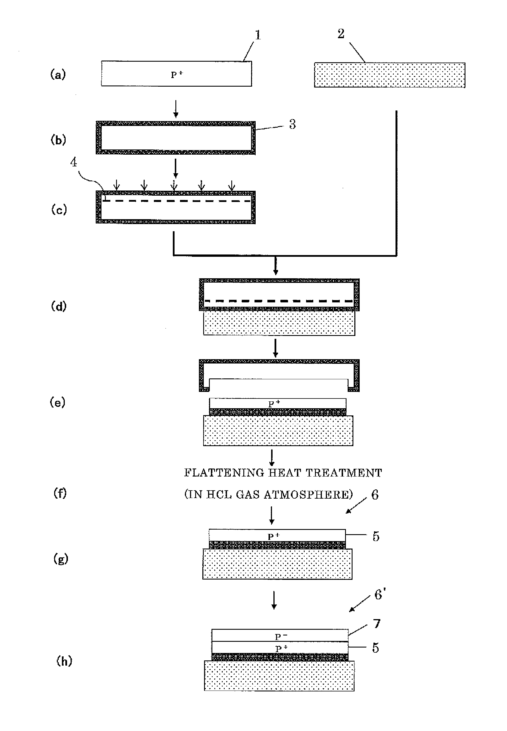
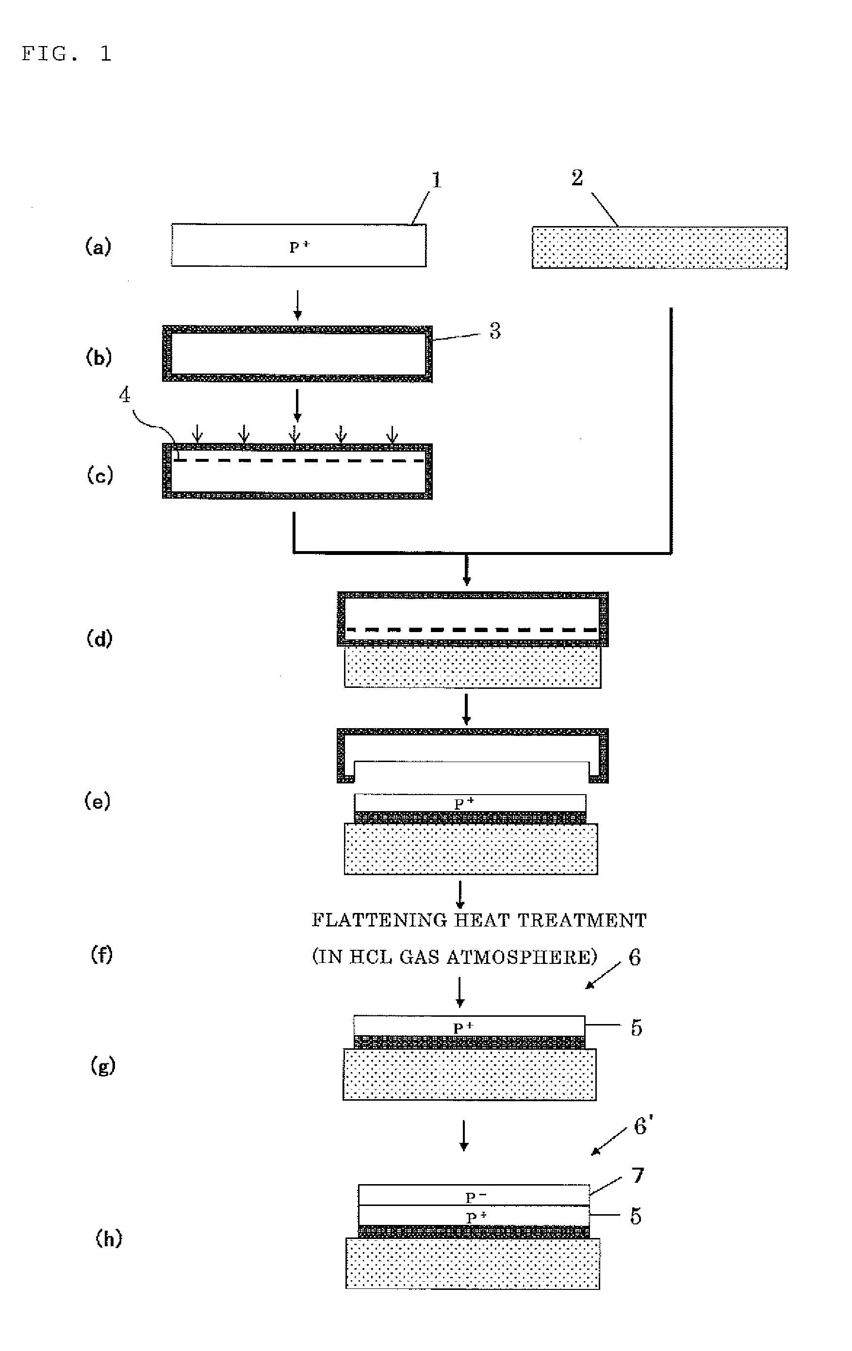
[0061]A p-type silicon single crystal wafer having an overall resistivity of 0.008 Ωcm (doped with boron at a concentration of 1.1×10¹⁹ / cm3) was prepared as the bond wafer, and ions were implanted into the bulk from its surface. The ion implanting conditions were as follows: a implantation energy of 50 keV; a dose of 4.0×10¹⁶ / cm2. Then, the bond wafer was bonded to a base wafer with a 150 nm thick thermal oxide film formed on its surface, and the delamination heat treatment was performed at 500° C. for 30 minutes to manufacture the SOT wafer. After the flattening heat treatment (gas etching with HCl) was performed in the same conditions as Example 1(a) and Example 1(b), the boron concentration on the SOI surface was measured with SIMS. The result is given in Table 3.

TABLE 3BOND WAFEREXAMPLEEXAMPLEEXAMPLE2340.016Ωcm0.008Ωcm0.008ΩcmOXIDATION SURFACEBONDBONDBASEWAFERWAFERWAFERBORON4.5e18 / cm31.1e19 / cm31.1e19 / cm3CONCENTRATIONOF SUBSTRATEION IMPLANTATION50 keV50 keV50 keVCONDITIONS4.0e16 / ...


PUM

PropertyMeasurementUnit
resistivityaaaaaaaaaa

Abstract

A method for manufacturing a bonded wafer including: forming an ion-implanted layer in a bond wafer, bonding the bond wafer to a base wafer, delaminating the bond wafer at the ion-implanted layer, and performing a flattening heat treatment on a surface after delamination, in which a silicon single crystal wafer is used as the bond wafer where the region to form the ion-implanted layer has a resistivity of 0.2 Ωcm or less, the ion-implanted layer is formed where the ion dose for forming the layer is 4×10¹⁶/cm2 or less, and the flattening heat treatment is performed in an atmosphere including HCl gas. Therefore, a method for manufacturing a bonded wafer having a low resistivity thin film (SOI layer) that contains dopant, such as boron, with high concentration according to the ion-implantation delamination method, where outward diffusion of dopant and suction due to oxidation can be inhibited to maintain low resistivity.

Description

TECHNICAL FIELD[0001]The present invention relates to a method for manufacturing a bonded wafer by using an ion implantation delamination method.BACKGROUND ART[0002]In a method for manufacturing bonded wafers by the ion implantation delamination method, surface roughness after delamination is insufficient and a damaged layer due to ion implantation remains on a surface after delamination; therefore it is necessary to improve the surface roughness and remove the damaged layer. As a method for improving surface roughness, a method of performing an annealing process under a hydrogen or inert gas atmosphere has been conventionally used to improve the surface roughness (See Patent Documents 1 and 2).[0003]As a method of improving surface roughness and simultaneously removing the damaged layer due to ion implantation, a CMP (Chemical Mechanical Polishing) process has been conventionally performed to improve the surface roughness and thin a film thickness. The CMP process deteriorates a ra...

Claims


Application Information

Patent Timeline
Patent Type & Authority Applications(United States)
IPC IPC(8): H01L21/265
CPCH01L21/76254H01L21/3247H01L21/3065H01L21/302H01L21/265
Inventor AGA, HIROJIOKA, SATOSHINOTO, NOBUHIKO
Owner SHIN-ETSU HANDOTAI CO LTD
Why Eureka
Try Eureka