Light emitting element

a technology of light-emitting elements and light-emitting components, which is applied in the direction of organic chemistry, solid-state devices, thermoelectric devices, etc., to achieve the effect of sufficient durability life and high light-emitting efficiency

Inactive Publication Date: 2013-05-02
TORAY IND INC
View PDF2 Cites 393 Cited by
  • Summary
  • Abstract
  • Description
  • Claims
  • Application Information

AI Technical Summary

Benefits of technology

[0023]This invention can provide an organic electric-field light-emitting element driven at lo

Problems solved by technology

However, there still remain many technical problems, and above all, one of large p

Method used


Image

  • Light emitting element
  • Light emitting element
  • Light emitting element

Examples


example 1

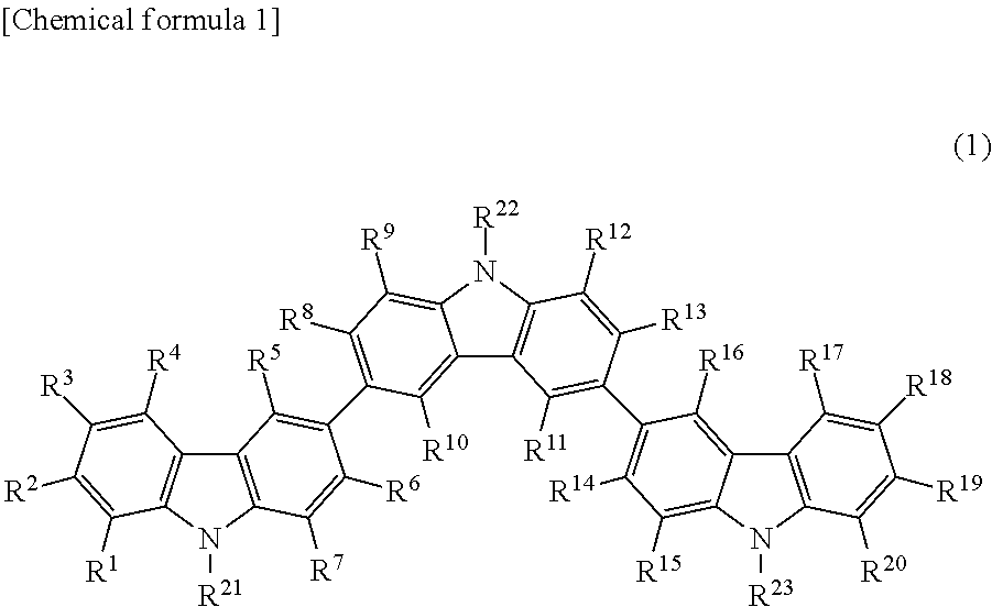
[0092]A glass substrate with 165 nm of an ITO transparent conductive film deposited (produced by Geomatec Co., Ltd., 11Ω / □, sputtered product) was cut to 38×46 mm, and etched. The obtained substrate was ultrasonically washed with “SEMICO CLEAN 56” (trade name, produced by Furuuchi Chemical Corporation) for 15 minutes, and washed with ultrapure water. The substrate was treated with UV-ozone for 1 hour immediately before the element was produced, and installed in a vacuum deposition apparatus. The air in the apparatus was exhausted to achieve a vacuum degree of 5×10⁴ Pa or less in the apparatus. A resistance heating method was used to vapor-deposit compound [1] as a hole transport layer by 60 nm. Then, using compound (H-1) as a host material and compound (D-1) as a dopant material, a light-emitting layer was vapor-deposited to achieve a dopant material doping concentration of 5 wt % and to have a thickness of 40 nm. Subsequently using compound (E-1) as an electron transport material a...

examples 2 to 8

[0094]Light-emitting elements were produced and evaluated as described in Example 1, except that the materials shown in Table 1 were used as a hole transport layer, light-emitting layer host material, light-emitting layer dopant material and second electron transport layer. The results of the respective examples are shown in Table 1. Meanwhile, compound (E-2) is the following compound.

example 7

[0095]A glass substrate with 165 nm of an ITO transparent conductive film deposited (produced by Geomatec Co., Ltd., 11Ω / □, sputtered product) was cut to 38×46 mm, and etched. The obtained substrate was ultrasonically washed with “SEMICO CLEAN 56” (trade name, produced by Furuuchi Chemical Corporation) for 15 minutes, and washed with ultrapure water. The substrate was treated with UV-ozone for 1 hour immediately before the element was produced, and installed in a vacuum deposition apparatus. The air in the apparatus was exhausted to achieve a vacuum degree of 5×10⁻⁴ Pa or less in the apparatus. A resistance heating method was used to vapor-deposit compound [1] as a hole transport layer by 60 nm. Then, using compound (H-1) as a host material and compound (D-1) as a dopant material, a light-emitting layer was vapor-deposited to achieve a dopant material doping concentration of 5 wt % and to have a thickness of 40 nm. Subsequently E-2 was vapor-deposited as a first electron transport l...


PUM


Abstract

Provided is an organic thin film light emitting element which has achieved all of improved luminous efficiency, improved driving voltage and improved durability life. Specifically provided is a light emitting element which comprises a hole transport layer and an electron transport layer between a positive electrode and a negative electrode and emits light by means of electrical energy. The light emitting element is characterized in that: the hole transport layer of the light emitting element contains a compound represented by general formula (1); the electron transport layer contains a donor compound; and the donor compound is an alkali metal, an inorganic salt containing an alkali metal, a complex of an alkali metal and an organic substance, an alkaline earth metal, an inorganic salt containing an alkaline earth metal, or a complex of an alkaline earth metal and an organic substance. (In the formula, R1-R20 each represents one group selected from the group consisting of hydrogen, deuterium, an alkyl group, a cycloalkyl group, an amino group, an aryl group, a heterocyclic group, a heteroaryl group, an alkenyl group, a cycloalkenyl group, an alkynyl group, analkoxy group, an alkylthio group, an arylether group, an arylthioether group, a halogen, a cyano group, a —P(═O)R24R25 group and a silyl group; R24 and R25 each represents an aryl group or a heteroaryl group; and these substituents may be further substituted, or adjacent two substituents may combine together to form a ring. Meanwhile, R21-R23 may be the same or different and each represents one group selected from the group consisting of an alkyl group, a cycloalkyl group, an aryl group and a heteroaryl group; and these substituents maybe further substituted.)

Description

TECHNICAL FIELD[0001]The present invention is a light-emitting element that can convert electric energy into light, and relates to a light-emitting element that can be used in the fields of display elements, flat panel displays, backlights, illumination, interior materials, signs, signboards, digital cameras, light signal generators, etc.BACKGROUND ART[0002]Research on organic thin-film light-emitting elements in which when the electrons injected from a cathode and the positive holes injected from an anode recombine in an organic fluorescent material, light is emitted is actively conducted in recent years. The light-emitting elements attract attention, since they are characterized by thin thickness, high-luminance light emission at low drive voltage and multi-color light emission obtained with selected fluorescent materials.[0003]C. W. Tang et al. (Kodak) demonstrated that organic thin-film elements emit light at high luminance, and since then, studies have been conducted by many re...

Claims


Application Information

Patent Timeline
IPC IPC(8): H01L51/00
CPCC07D209/86H01L51/5056H01L51/5004H01L51/0072H10K85/6572H10K50/11H10K2101/40H10K50/15
Inventor TANAKA, DAISAKUMATSUKI, SHINICHITOMINAGA, TSUYOSHI
Owner TORAY IND INC
Why Eureka
Try Eureka