Thin-film transistor

Inactive Publication Date: 2013-05-09
ADVANCED INTERCONNECT MATERIAL
View PDF2 Cites 23 Cited by
  • Summary
  • Abstract
  • Description
  • Claims
  • Application Information

AI Technical Summary

Benefits of technology

[0043]In accordance with the present invention, the provision of an oxide reaction layer between the semiconductor layer comprising the oxide semiconductor and, respectively, makes it possible to improve adhesion between the source electrode and the semiconductor layer and adhesion between the drain electrode and the semiconductor layer.
[0044]Further, the thin-film transistor can achieve high-speed operation because the semiconductor layer comes to acquire low-resistance ohmic contact to the source electrode and the drain electrode through the oxide reac

Problems solved by technology

However, in addition to being poor in adhesion to the TFT substrate of an LCD, that is glass, copper also has a problem of being easily oxidized during insulation layer formation.
However, the sought characteristics are not adequately achieved by the proposed technology.
However, this technology has problems in that a Mo alloy film-forming process is added and the effective resistance of the interconnections increases.
In addition, Cu-only layers are used at the source electrode and drain electrode, so that an issue of their stability remains.
However, as compared to a conventional interconnection material, this technology has problems in that a material for forming a barrier layer and an additional process are required, and that the effective resistance of the interconnections rises because the high-resistance barrier layer is formed to thick film thickness.
However, increase in interconnection resistance owing to the presence of residual additive

Method used


Image

  • Thin-film transistor
  • Thin-film transistor
  • Thin-film transistor

Examples


Embodiment Construction

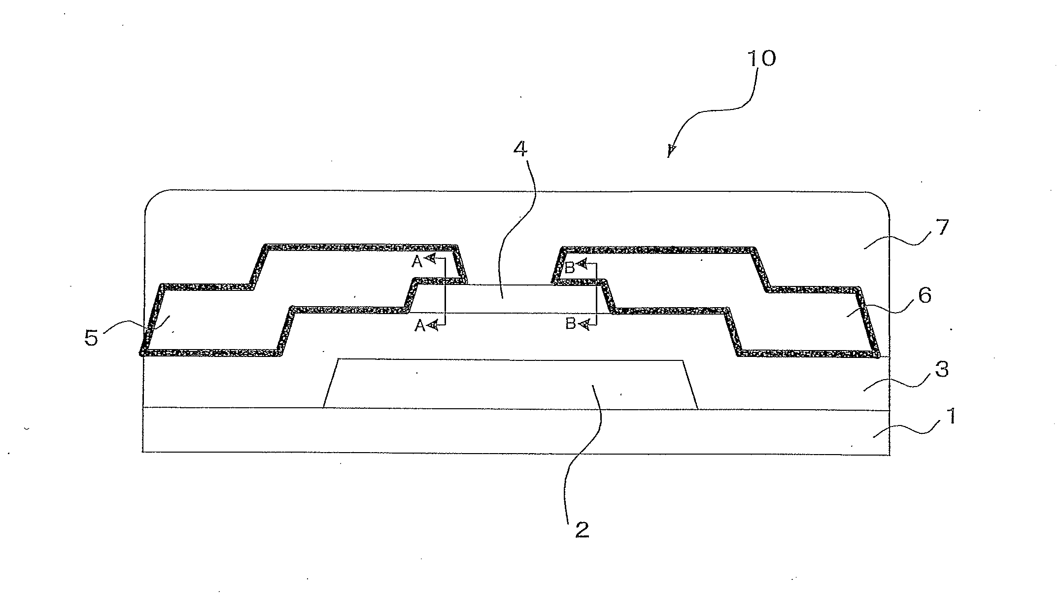
[0063]An embodiment of this invention will be described in detail below. FIG. 1 is a diagram showing the cross-sectional structure of a thin-film transistor according to the present invention. The thin-film transistor (TFT) 10 in FIG. 1 functions as a drive device that performs display driving of, for example, a liquid crystal display, organic EL (Electro Luminescence) display or the like, and has a bottom gate structure, for example.

[0064]The thin-film transistor 10 has a gate electrode 2 at a selected region on a substrate 1 composed of glass, plastic or the like. A gate insulating film 3 is formed so as to cover the gate electrode 2 and substrate 1. A semiconductor layer 4 is provided on the gate insulating film 3, and a source electrode 5 and a drain electrode 6 are arranged locally on the semiconductor layer 4 in a predetermined pattern. And a protective film (passivation film) 7 is overlaid on the source electrode 5, drain electrode 6, and semiconductor layer 4.

[0065]The gate ...


PUM


Abstract

Making it possible to improve adhesion between the semiconductor layer and the electrodes, realize high-speed operation of the thin-film transistor by enhancing ohmic contact between these members, reliably prevent oxidation of the electrode surfaces, and realize an electrode fabrication process with few processing steps. The thin-film transistor 10 of the present invention includes a semiconductor layer 4 composed of oxide semiconductor, a source electrode 5 and a drain electrode 6 that are layers composed mainly of copper, and oxide reaction layers 22 provided between the semiconductor layer 4 and each of the source electrode 5 and drain electrode 6, and high-conductance layers 21 provided between the oxide reaction layers 22 and semiconductor layer 4.

Description

TECHNICAL FIELD[0001]This invention relates to a thin-film transistor provided with an oxide semiconductor in the semiconductor layer.BACKGROUND ART[0002]Application of oxide semiconductors to thin-film transistors and transparent electrodes has attracted attention in recent years. Thin-film transistors that utilize oxide semiconductors are being actively applied to flat panel display devices like liquid crystal display devices and organic EL display devices. Moreover, transparent electrodes that utilize oxide semiconductors are being actively applied to flat panel display devices and touch panels.[0003]In these fields of application, materials of low resistance and high electrical conductivity are used in the interconnections and electrodes of the oxide semiconductor.[0004]In these fields of application, aluminum (Al) or Al alloy, molybdenum, and the like are used.[0005]For example, an interconnection material composed of Ti / Al—Si / Ti has been proposed that has a structure of Al—Si ...

Claims


Application Information

Patent Timeline
IPC IPC(8): H01L29/786
CPCH01L29/45H01L29/78693H01L29/7869
Inventor KOIKE, JUNICHIYUN, PILSANGKAWAKAMI, HIDEAKI
Owner ADVANCED INTERCONNECT MATERIAL
Why Eureka
Try Eureka