Prevention of ILD Loss in Replacement Gate Technologies by Surface Treatmen

a technology of surface treatmen and replacement gate, which is applied in the field of integrated circuits, can solve the problems of significant variability of the resulting work function and thus threshold voltage of the completed transistor structure, increase of layer thickness and thus a reduction of capacitive coupling, and achieve the effect of improving the surface characteristics of superior surface topography in the interlayer dielectric material, and enhancing etch resistivity

Inactive Publication Date: 2013-05-09
GLOBALFOUNDRIES INC
View PDF7 Cites 17 Cited by
  • Summary
  • Abstract
  • Description
  • Claims
  • Application Information

AI Technical Summary

Benefits of technology

[0023]Generally, the present disclosure provides manufacturing techniques in which a superior surface topography in the interlayer dielectric material may be obtained upon removing a placeholder material by improving the surface characteristics of the interlayer dielectric material prior to applying one or more critical process steps of the replacement gate approach. In some illustrative aspects disclosed herein, a surface modification may be applied to an exposed surface of the interlayer dielectric material at least once prior to completely removing the placeholder material, thereby imparting at least enhanced etch resistivity to the interlayer dielectric material, however, without unduly modifying the overall dielectric characteristics of the interlayer dielectric material. To this end, a plurality of surface modification techniques, such as plasma treatments, chemical treatments and the like, may be efficiently applied, wherein the effect and the depth of modification may be readily adjusted on the basis of selecting appropriate process parameters.

Problems solved by technology

Hence, the conductivity of the channel region substantially affects the performance of MOS transistors.
Providing different metal species for adjusting the work function of the gate electrode structures for P-channel transistors and N-channel transistors at an early manufacturing stage may, however, be associated with a plurality of difficulties, which may stem from the fact that a complex patterning sequence may be required during the formation of the sophisticated high-k metal gate stack, which may result in a significant variability of the resulting work function and thus threshold voltage of the completed transistor structures.
For instance, during a corresponding manufacturing sequence, the high-k material may be exposed to oxygen, which may result in an increase of layer thickness and thus a reduction of the capacitive coupling.
Although in general this approach provides advantages in view of reducing process-related non-uniformities with respect to the threshold voltages of the transistors, since the sensitive metal species for adjusting the work function of the gate electrode structures may be provided after any high temperature processes, the complex process sequence for exposing and replacing the placeholder material may result in a pronounced yield loss, as will be explained in more detail with reference to FIGS. 1a-1d.
Although basically the etch strategies are highly selective, nevertheless a pronounced material erosion may occur in the interlayer dielectric material 120, which may thus result in a non-desired surface topography upon removing the polysilicon material 162.

Method used


Image

  • Prevention of ILD Loss in Replacement Gate Technologies by Surface Treatmen
  • Prevention of ILD Loss in Replacement Gate Technologies by Surface Treatmen
  • Prevention of ILD Loss in Replacement Gate Technologies by Surface Treatmen

Examples


Embodiment Construction

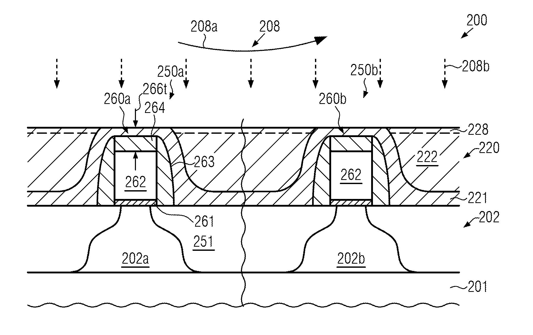
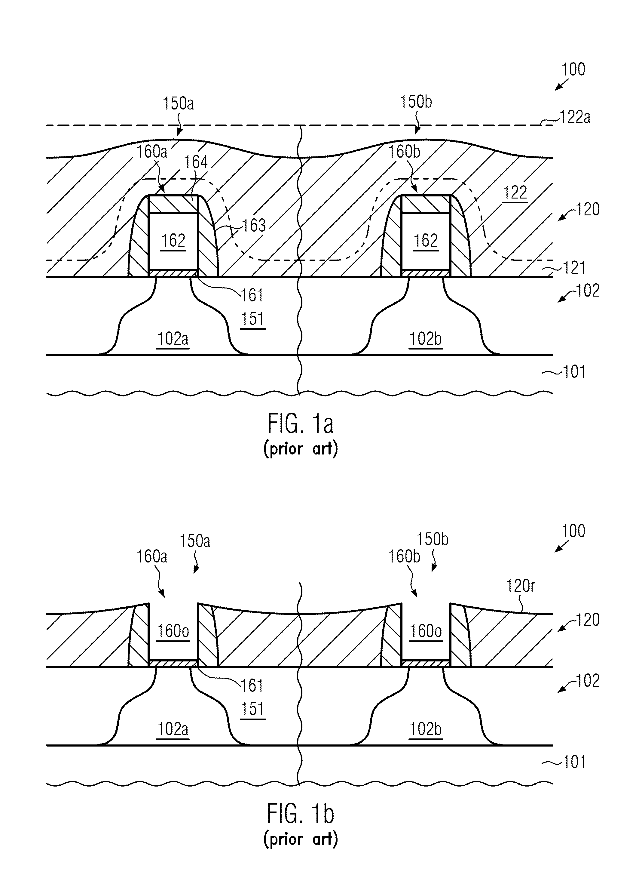
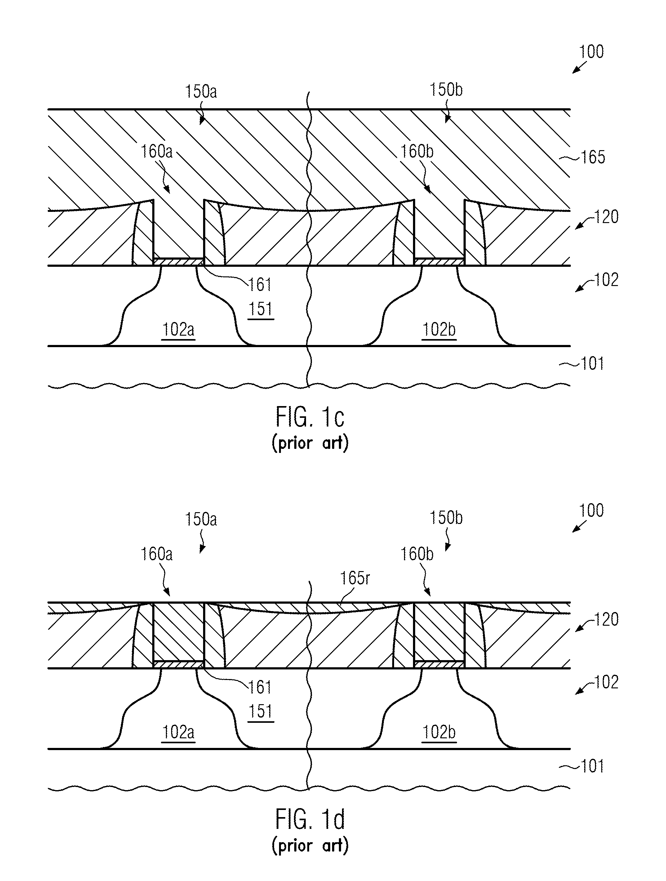
[0034]Various illustrative embodiments of the invention are described below. In the interest of clarity, not all features of an actual implementation are described in this specification. It will of course be appreciated that in the development of any such actual embodiment, numerous implementation-specific decisions must be made to achieve the developers' specific goals, such as compliance with system-related and business-related constraints, which will vary from one implementation to another. Moreover, it will be appreciated that such a development effort might be complex and time-consuming, but would nevertheless be a routine undertaking for those of ordinary skill in the art having the benefit of this disclosure.

[0035]The present subject matter will now be described with reference to the attached figures. Various structures, systems and devices are schematically depicted in the drawings for purposes of explanation only and so as to not obscure the present disclosure with details ...


PUM

PropertyMeasurementUnit
channel lengthaaaaaaaaaa
thicknessaaaaaaaaaa

Abstract

When forming sophisticated high-k metal gate electrode structures on the basis of a replacement gate approach, pronounced loss of the interlayer dielectric material may be avoided by inserting at least one surface modification process, for instance in the form of a nitridation process. In this manner, leakage paths caused by metal residues formed in the interlayer dielectric material may be significantly reduced.

Description

BACKGROUND OF THE INVENTION[0001]1. Field of the Invention[0002]Generally, the present disclosure relates to integrated circuits including transistors with gate electrode structures formed on the basis of replacement gate technology.[0003]2. Description of the Related Art[0004]The fabrication of advanced integrated circuits, such as CPUs, storage devices, ASICs (application specific integrated circuits) and the like, requires the formation of a large number of circuit elements on a given chip area according to a specified circuit layout, wherein field effect transistors represent one important type of circuit element that substantially determines performance of the integrated circuits. Generally, a plurality of process technologies are currently practiced, wherein, for many types of complex circuitry, including field effect transistors, CMOS technology is one of the most promising approaches due to the superior characteristics in view of operating speed and / or power consumption and / ...

Claims


Application Information

Patent Timeline
Patent Type & Authority Applications(United States)
IPC IPC(8): H01L21/311
CPCH01L21/84H01L21/3105H01L21/31155H01L21/823412H01L29/7833H01L21/823437H01L21/823807H01L21/823828H01L29/66545H01L21/823425
Inventor PAL, ROHITSTEPHAN, ROLFOTT, ANDREAS
Owner GLOBALFOUNDRIES INC
Why Eureka
Try Eureka