Display device and manufacturing method thereof

a liquid crystal display and manufacturing method technology, applied in semiconductor devices, optics, instruments, etc., can solve the problems of increased manufacturing cost, increased number of manufacturing steps, and high cost of photolithography masks, and achieve and high-reliability liquid crystal display devices

Inactive Publication Date: 2013-05-16
SEMICON ENERGY LAB CO LTD
View PDF4 Cites 22 Cited by
  • Summary
  • Abstract
  • Description
  • Claims
  • Application Information

AI Technical Summary

Benefits of technology

[0007]For transistors used in a liquid crystal display device, it is preferable that change in electric characteristics (such as threshold voltage, mobility, or S value) due to deterioration over time be small and variation in electric characteristics due to deterioration over time be small. With use of transistors in which change in electric characteristics due to deterioration over time is small or transistors in which variation in electric characteristics due to deterioration over time is small, reliability of the liquid crystal display device can be improved, and quality of displayed images can be enhanced.
[0008]A mask for light exposure, which is used in a photolithography method, is generally expensive. In addition, in a photolithography method, a series of steps including formation of a photoresist, exposure, development, etching, separation, and the like is needed for one mask. Thus, as the number of masks needed for manufacturing the liquid crystal display device is increased, the number of manufacturing steps is increased, and manufacturing cost is increased.
[0009]In view of the foregoing technical background, an object of the present invention is to provide a highly reliable liquid crystal display device. Another object of the present invention is to provide a highly reliable liquid crystal display device which can be manufactured with use of a small number of masks.

Problems solved by technology

A mask for light exposure, which is used in a photolithography method, is generally expensive.
Thus, as the number of masks needed for manufacturing the liquid crystal display device is increased, the number of manufacturing steps is increased, and manufacturing cost is increased.

Method used


Image

  • Display device and manufacturing method thereof
  • Display device and manufacturing method thereof
  • Display device and manufacturing method thereof

Examples


embodiment 1

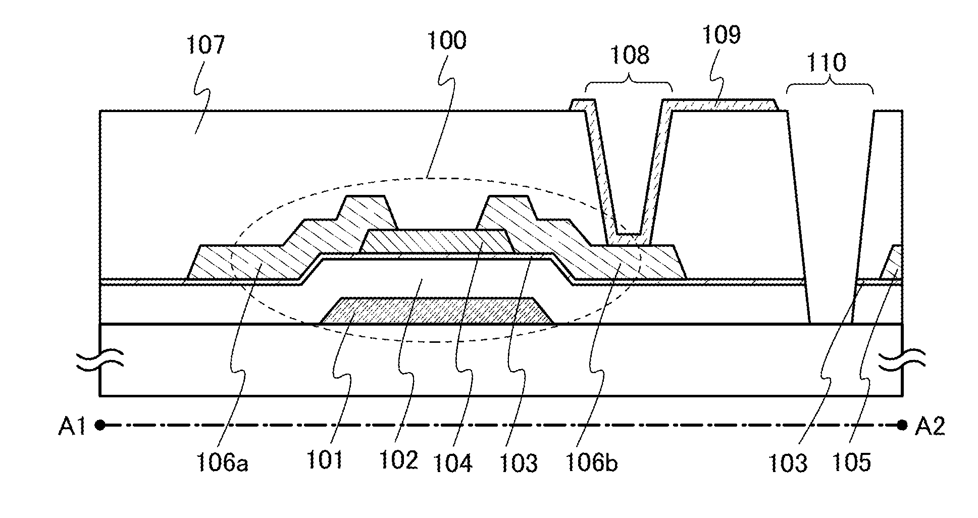
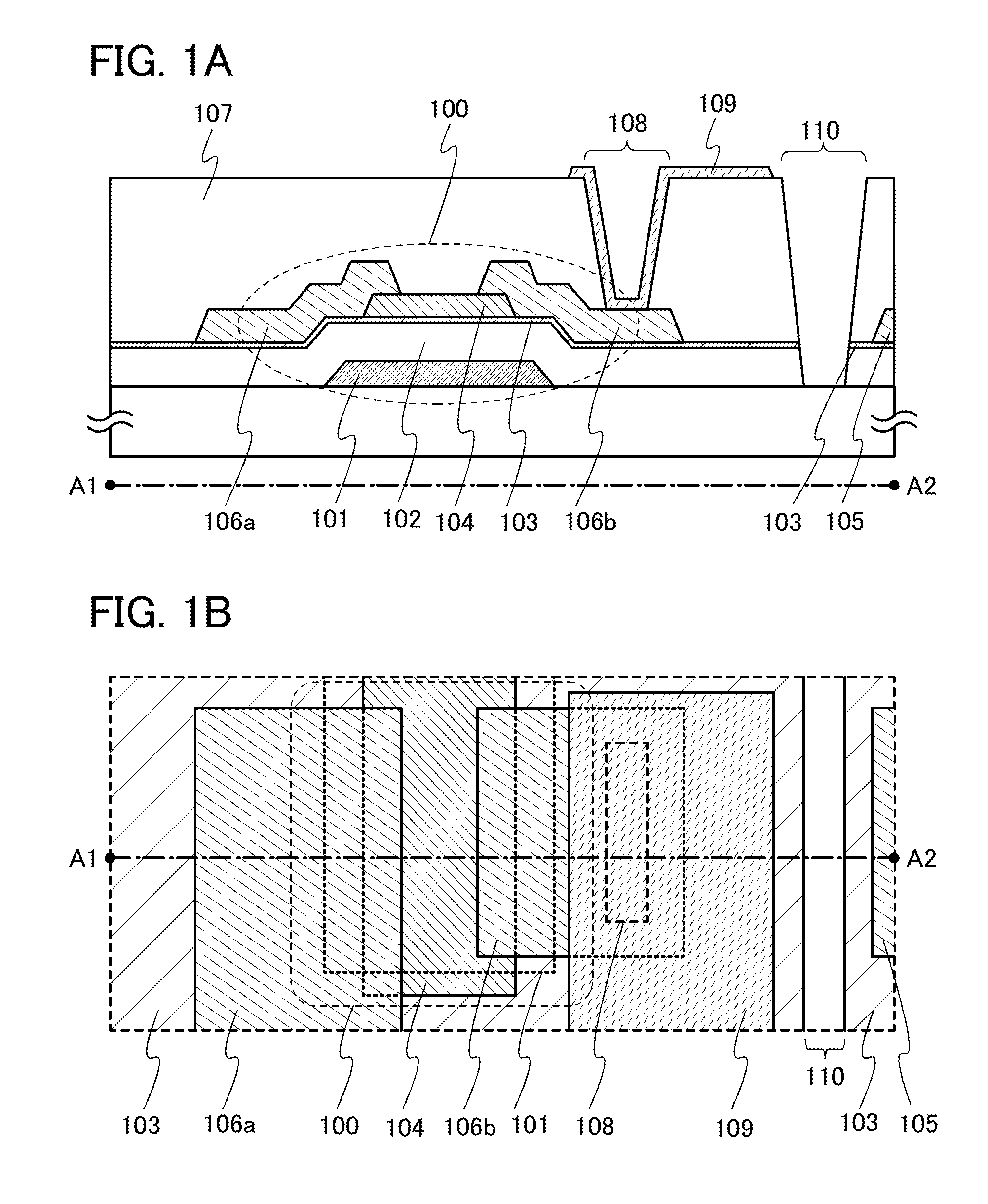
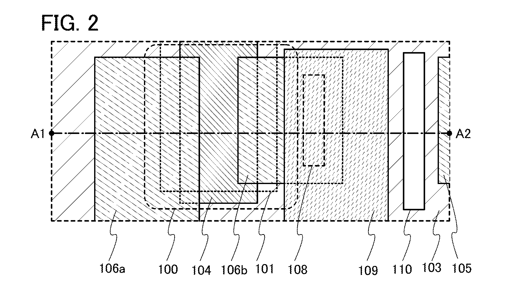
[0064]FIGS. 1A and 1B illustrate a structure of a liquid crystal display device according to one embodiment of the present invention. FIG. 1A is an example of a cross-sectional view in the channel length direction of a transistor 100 included in a pixel.

[0065]FIG. 1A illustrates the following components: a gate electrode 101 over an insulating surface; a gate insulating film 102 provided over the gate electrode 101; a semiconductor film 103 which is provided over the gate insulating film 102 and overlaps with the gate electrode 101; an island-shaped insulating film 104 which is provided over the semiconductor film 103 and overlaps with the gate electrode 101; a conductive film 105 provided over the semiconductor film 103; a conductive film 106a and a conductive film 106b which are provided over the semiconductor film 103 and between which the insulating film 104 is sandwiched; an insulating film 107 provided over the semiconductor film 103, the insulating film 104, the conductive fi...

embodiment 2

[0109]Next, an example of a specific structure of a pixel portion of a liquid crystal display device according to one embodiment in the present invention will be described.

[0110]FIG. 8A illustrates a structure example of a pixel portion 10. In FIG. 8A, y scan lines GL (GL1 to GLy) whose potentials are controlled by a scan line driver circuit and x signal lines SL (SL1 to SLx) whose potentials are controlled by a signal line driver circuit are provided in the pixel portion 10.

[0111]The scan lines GL are connected to a plurality of pixels 11. Specifically, each scan line GL is connected to x pixels 11 in a given row, among the plurality of pixels 11 arranged in matrix.

[0112]Each signal line SL is connected to y pixels 11 in a given column, among the plurality of pixels 11 arranged in matrix of x columns and y rows in the pixel portion 10.

[0113]Note that the term “connection” in this specification refers to electrical connection and corresponds to the state in which current, potential,...

embodiment 3

[0142]In this embodiment, a method for manufacturing a liquid crystal display device according to one embodiment of the present invention will be described, with use of the pixel 11 illustrated in FIG. 5 and FIGS. 6A and 6B as an example.

[0143]First, as illustrated in FIG. 9A, over the substrate 202 having an insulating surface, the conductive film 203 functioning as a gate electrode and the conductive film 210 functioning as an electrode of the capacitor 14 are formed.

[0144]Although there is no particular limitation on a substrate that can be used as the substrate 202 having an insulating surface, the substrate needs to have heat resistance high enough to withstand at least heat treatment to be performed later. For example, a glass substrate manufactured by a fusion process or a float process can be used. In addition, when the temperature of the heat treatment performed later is high, a glass substrate having a strain point of 730° C. or higher is preferably used. As a glass substr...


PUM


Abstract

The display device includes a gate electrode, a gate insulating film provided over the gate electrode, a semiconductor film provided over the gate insulating film to overlap with the gate electrode, an island-shaped first insulating film provided over the semiconductor film to overlap with the gate electrode, a first conductive film provided over the semiconductor film, a pair of second conductive films which is provided over the semiconductor film and between which the first insulating film is sandwiched, and a second insulating film provided over the first insulating film, the first conductive film, and the pair of second conductive films. In the second insulating film and the semiconductor film, an opening portion which is positioned between the first conductive film and the one or the other of the pair of second conductive films is provided.

Description

BACKGROUND OF THE INVENTION[0001]1. Field of the Invention[0002]The present invention relates to a liquid crystal display device in which transistors are provided in respective pixels, and a manufacturing method thereof. The present invention also relates to a light-emitting display device in which transistors are provided in respective pixels, and a manufacturing method thereof.[0003]2. Description of the Related Art[0004]In recent years, a metal oxide having semiconductor characteristics, which is called an oxide semiconductor, has attracted attention as a novel semiconductor material having both high mobility almost the same as that of crystalline silicon and uniform element characteristics almost the same as those of amorphous silicon. The metal oxide is used for a variety of applications. For example, indium oxide is a well-known metal oxide and used as a material of a light-transmitting pixel electrode included in a liquid crystal display device or the like. Examples of such m...

Claims


Application Information

Patent Timeline
Patent Type & Authority Applications(United States)
IPC IPC(8): G02F1/1333H01L33/08H01L27/15
CPCH01L27/1225H01L27/1255G02F2001/136231G02F1/1368H01L27/1259G02F1/136231H01L27/1248G02F1/136227H01L29/66969H01L29/78606H01L29/7869
Inventor YAMAZAKI, SHUNPEIKOYAMA, JUN
Owner SEMICON ENERGY LAB CO LTD
Why Eureka
Try Eureka