Submount for light emitting diode and method for fabricating the same
- Summary
- Abstract
- Description
- Claims
- Application Information
AI Technical Summary
Benefits of technology
Problems solved by technology
Method used
Image
Examples
first embodiment
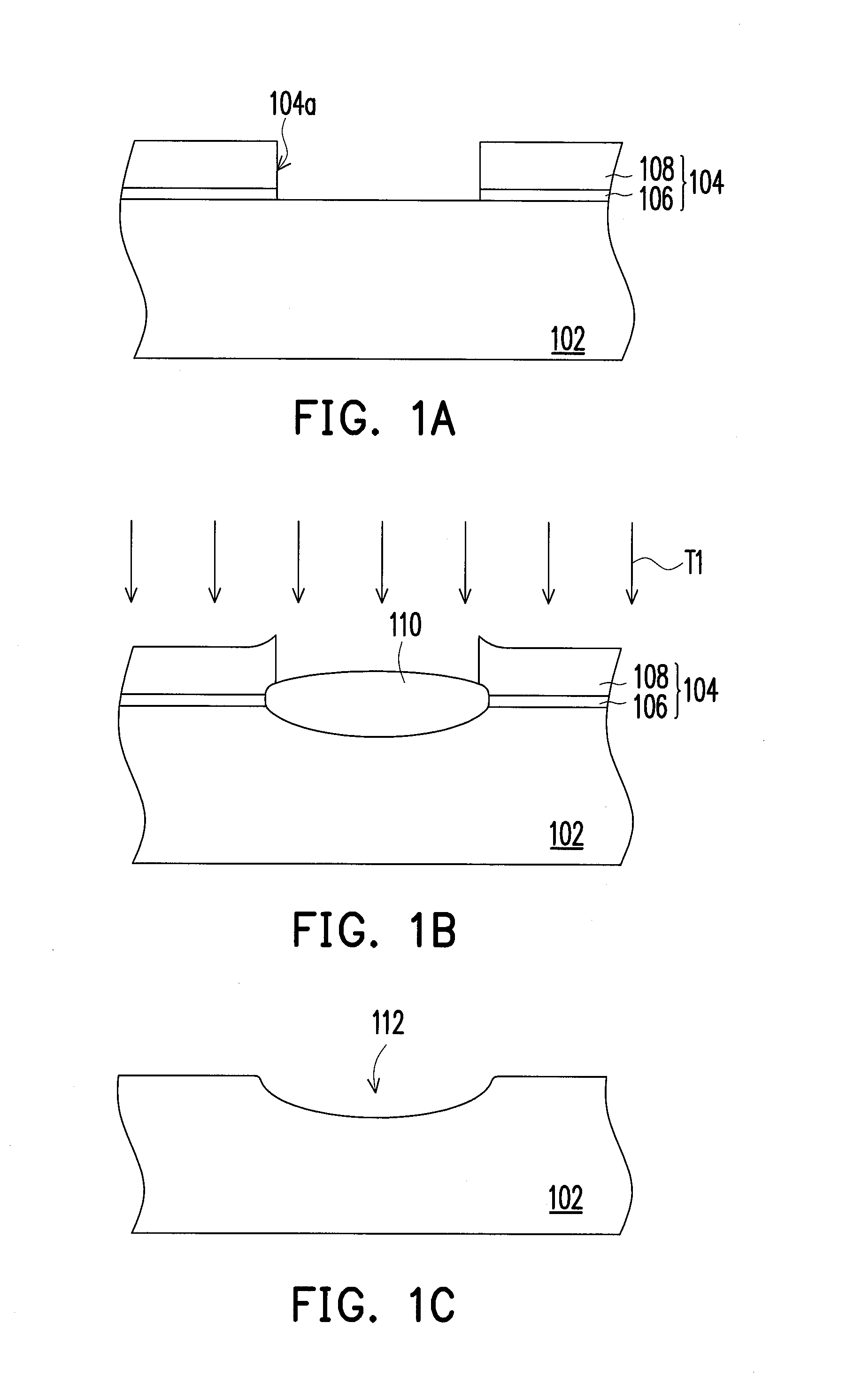
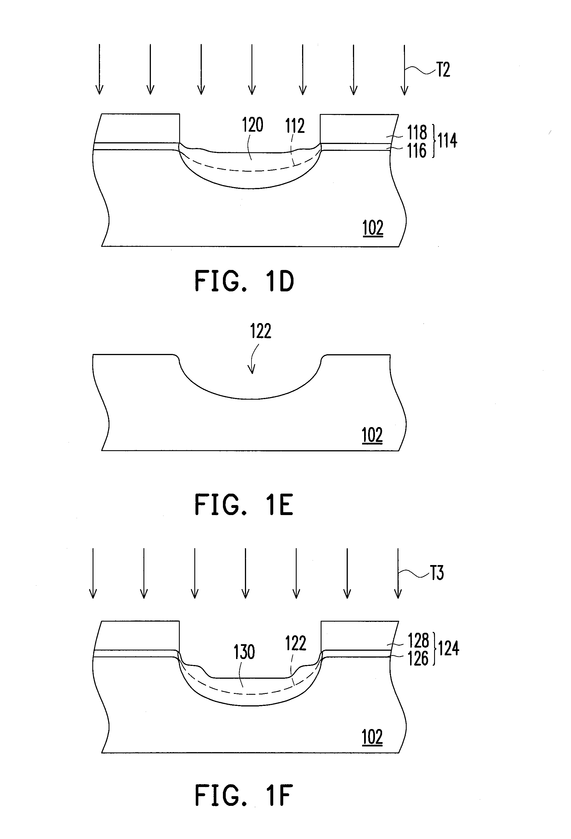
[0035]FIG. 1A to FIG. 1H are schematic cross-sectional views illustrating a method for fabricating a submount for an LED according to the present invention. FIG. 2 is a schematic three-dimensional view illustrating a recess in the structure of the submount for the LED in FIG. 1H, wherein a reflective layer and an LED chip are omitted.
[0036]Referring to FIG. 1A, a silicon substrate 102 is provided and a mask layer 104 is formed on the silicon substrate 102. The mask layer 104 has an opening 104a that exposes a part of a surface of the silicon substrate 102, so as to define an area where the recess is to be formed subsequently. In the embodiment, the mask layer 104 includes a pad oxide layer 106 and a silicon nitride layer 108. The pad oxide layer 106 is located between the silicon substrate 102 and the silicon nitride layer 108 to increase the adhesion between the silicon nitride layer 108 and the silicon substrate 102. The pad oxide layer 106 may be formed by adopting a thermal oxid...
second embodiment
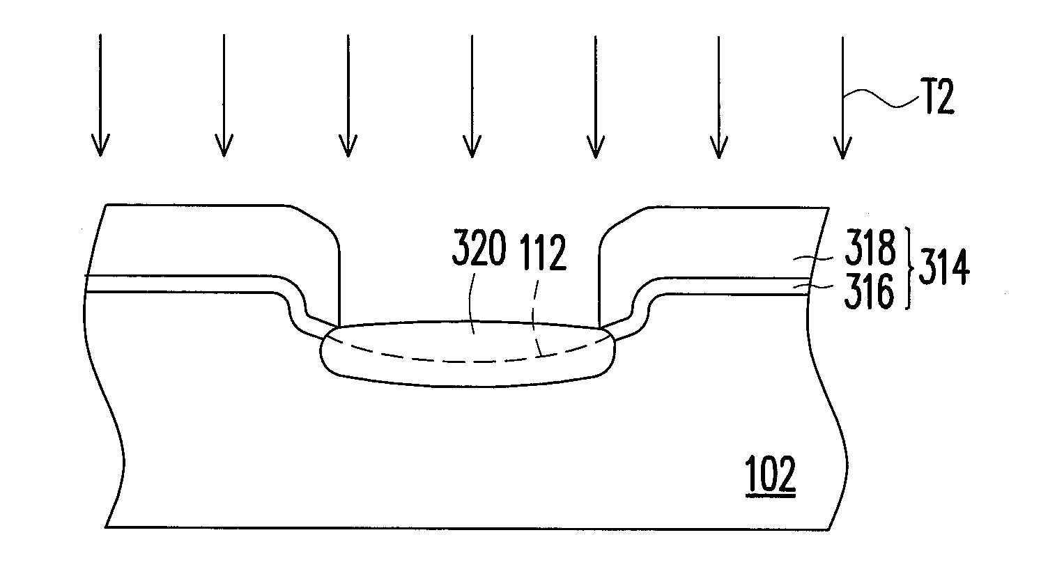
[0051]FIG. 3A to FIG. 3E are schematic cross-sectional views illustrating a method for fabricating a submount for an LED according to the present invention. The fabrication steps in FIG. 3A are subsequent to steps in FIG. 1C, and the same members are indicated by the same reference numerals and the illustration of the members is omitted. FIG. 4 is a schematic three-dimensional view illustrating a recess in the structure of the submount for the LED in FIG. 3E, wherein the reflective layer and the LED chip are omitted.
[0052]Referring to FIG. 3A, after the recess 112 is formed, a mask layer 314 is formed on the silicon substrate 102 again, and the mask layer 314, for example, exposes a part of the surface of the silicon substrate 102 located at the recess 112. In an embodiment, the range of the silicon substrate 102 exposed by the mask layer 314 is, for example, smaller than the range of the silicon substrate 102 exposed by the mask layer 104 in FIG. 1A. In other words, the mask layer ...
third embodiment
[0061]FIG. 5A to FIG. 5D are schematic cross-sectional views illustrating a method for fabricating a submount for an LED according to the present invention. The fabrication steps in FIG. 5A are subsequent to the steps in FIG. 1G, and the same components are indicated by the same reference numerals and the illustration of the components is omitted. FIG. 6 is a schematic three-dimensional view illustrating a recess in the structure of the submount for the LED in FIG. 5D, wherein the reflective layer and the LED chip are omitted.
[0062]Referring to FIG. 5A, after the recess 132 is formed, an ion implantation process I is performed to form a plurality of implantation regions 502 in a part of the sidewall of the recess 132. In an embodiment, the ion implantation process I, for example, implants oxygen ions in the substrate 102. Furthermore, the ion implantation process I may be used together with a patterned photoresist to define the implantation area and vertical implantation or inclined...
PUM
 Abstract
Description
Claims
Application Information


