Carbon Nanotube-Graphene Hybrid Transparent Conductor and Field Effect Transistor

a carbon nanotube and conductor technology, applied in nanoinformatics, transportation and packaging, natural mineral layered products, etc., can solve the problems of underperformance of alternative tc coatings in terms of transparency and sheet resistance, and achieve the effect of improving electrical performance and decreasing nanotubes

Active Publication Date: 2013-05-23
IBM CORP +1
View PDF6 Cites 59 Cited by
  • Summary
  • Abstract
  • Description
  • Claims
  • Application Information

AI Technical Summary

Benefits of technology

[0004]In one aspect of the invention, a method for forming a cleaned nanotube-graphene hybrid film is provided. The method includes the steps of depositing nanotube film over a substrate to produce a layer of nanotube film, removing impurities from a surface of the layer of nanotube film not contacting the substrate to produce a cleaned layer of nanotube film, depositing a layer of graphene over the cleaned layer of nanotube film to produce a nanotube-graphene hybrid film, and removing impurities from a surface of the nanotube-graphene hybrid film to produce a cleaned nanotube-graphene hybrid film, wherein the hybrid film has improved electrical performance via decreasing nanotube resistance by increasing contact area through use of graphene as a bridge.

Problems solved by technology

Indium tin oxide (ITO) and other amorphous TCs (fluorine doped zinc oxide, etc.) also have problems with use in the flexible electronic industry.
However, these alternatives still fall short of the required performance for TC coatings in terms of transparency and sheet resistance.

Method used


Image

  • Carbon Nanotube-Graphene Hybrid Transparent Conductor and Field Effect Transistor
  • Carbon Nanotube-Graphene Hybrid Transparent Conductor and Field Effect Transistor
  • Carbon Nanotube-Graphene Hybrid Transparent Conductor and Field Effect Transistor

Examples


Embodiment Construction

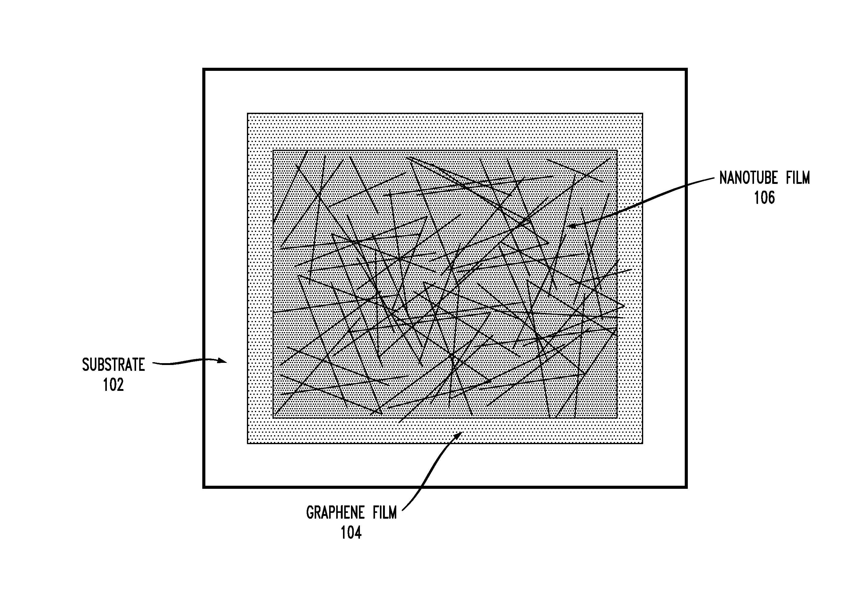
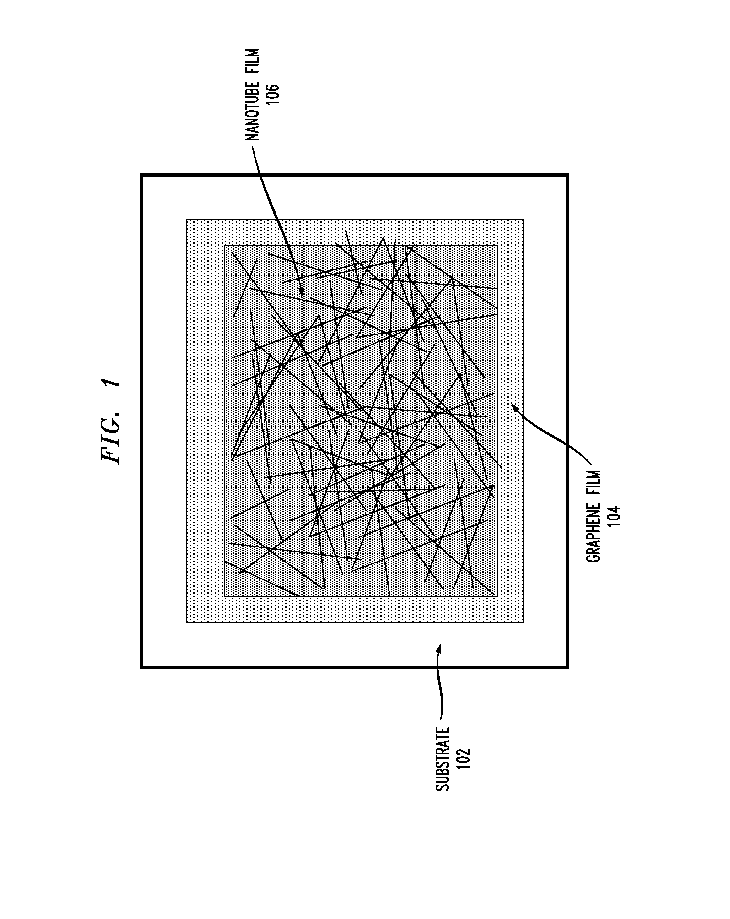
[0024]An aspect of the invention includes a carbon nanotube (CNT)-graphene hybrid as a transparent conductor. As detailed herein, an embodiment of the invention uses CNTs to improve the performance of graphene transparent electrodes. For example, an aspect of the invention includes a combination of thin films of nanotube and graphene, where the thin films of nanotubes are deposited over graphene or vice versa. Additionally, this combination can be used in coatings for transparent conductors (TCs).

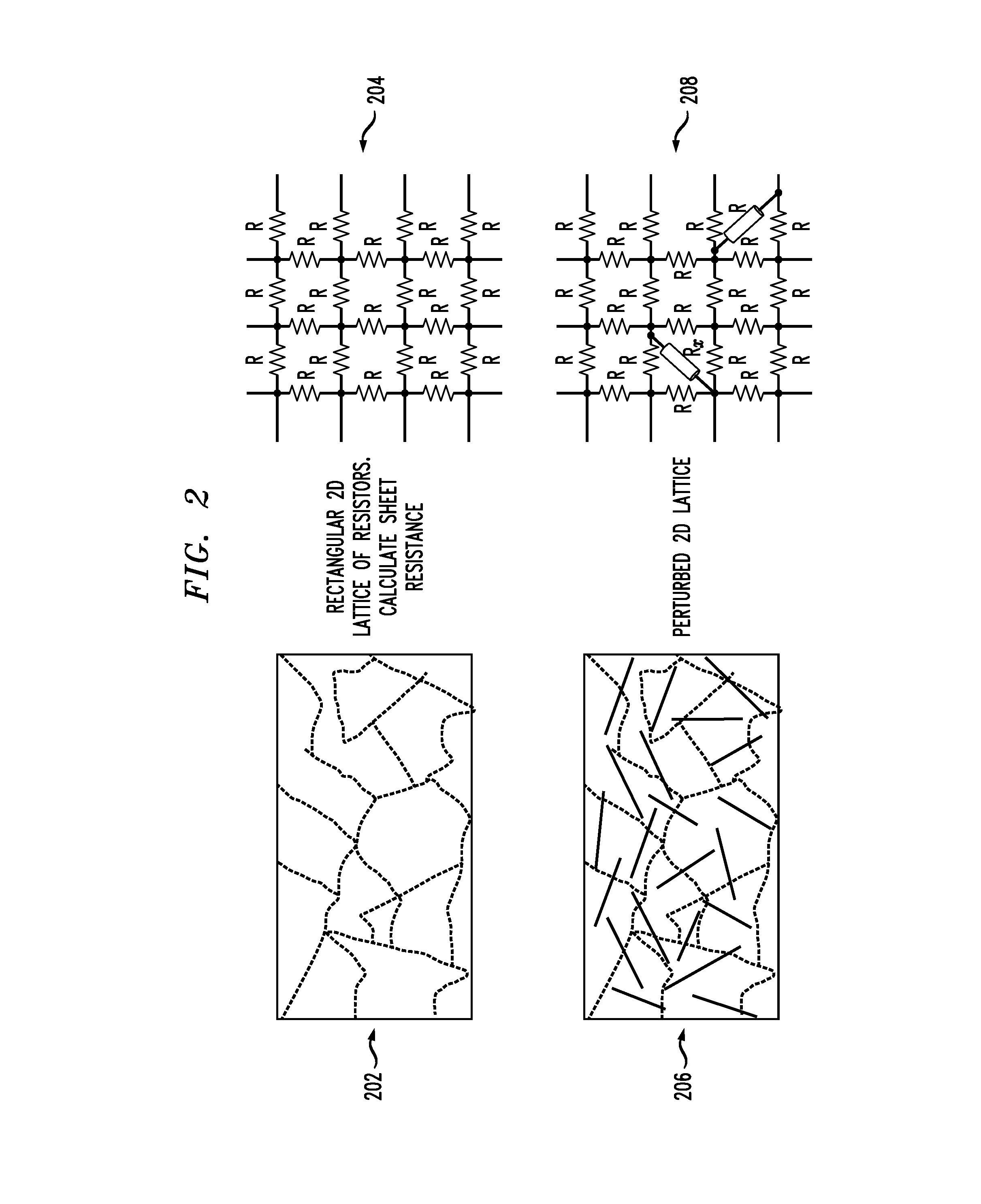
[0025]In an aspect of the invention, the electrical performance of thin films of nanotube and graphene is improved by depositing thin films of nanotubes over graphene or vice versa. As detailed herein, this arrangement decreases the tube-tube resistance by increasing the contact area through the use of graphene as a bridge. Also, nanotubes act as a bridge across the grain boundary scattering sites of graphene, thereby increasing the graphene conductivity. Additionally, in contrast to existi...


PUM

PropertyMeasurementUnit
temperaturesaaaaaaaaaa
temperatureaaaaaaaaaa
thicknessaaaaaaaaaa

Abstract

A nanotube-graphene hybrid film and method for forming a cleaned nanotube-graphene hybrid film. The method includes depositing nanotube film over a substrate to produce a layer of nanotube film, removing impurities from a surface of the layer of nanotube film not contacting the substrate to produce a cleaned layer of nanotube film, depositing a layer of graphene over the cleaned layer of nanotube film to produce a nanotube-graphene hybrid film, and removing impurities from a surface of the nanotube-graphene hybrid film to produce a cleaned nanotube-graphene hybrid film, wherein the hybrid film has improved electrical performance. Another method includes depositing nanotube film over a metal foil to produce a layer of nanotube film, placing the metal foil with as-deposited nanotube film in a chemical vapor deposition furnace to grow graphene on the nanotube film to form a nanotube-graphene hybrid film, and transferring the nanotube-graphene hybrid film over a substrate.

Description

FIELD OF THE INVENTION [0001]Embodiments of the invention generally relate to electronic devices and, more particularly, to transparent conductors.BACKGROUND OF THE INVENTION[0002]The ever-increasing cost of indium, a rare earth element used in coatings for transparent conductors (TCs), has given an impetus for research into several alternatives for use as a TC. Indium tin oxide (ITO) and other amorphous TCs (fluorine doped zinc oxide, etc.) also have problems with use in the flexible electronic industry.[0003]In recent years, carbon nanotube films and graphene have emerged as potential replacements for ITO as a TC in various technological applications such as photovoltaic devices, electronic displays, etc. However, these alternatives still fall short of the required performance for TC coatings in terms of transparency and sheet resistance. Accordingly, a need exists for effective alternatives for TC coating.SUMMARY OF THE INVENTION[0004]In one aspect of the invention, a method for ...

Claims


Application Information

Patent Timeline
Patent Type & Authority Applications(United States)
IPC IPC(8): B32B9/04C23F1/02B05D1/02C23C16/26B05D5/12B05D3/02B82Y30/00B82Y40/00
CPCH01L51/0048Y10T428/30H01L51/105H01L29/0673H01L29/1606C01B31/0453C01B31/0476C23C16/26H01B1/04H01L51/0566H01L51/102H01L29/778H01L29/66742H01L29/78618H01L29/78684H01L29/78696B82Y40/00B82Y10/00B82Y30/00H01L51/0545C01B32/186C01B32/192C01B2204/00C01B2202/00Y10S977/742Y10S977/75Y10S977/938H10K85/221H10K10/486H10K10/488H10K10/82H10K10/84H10K10/466H01L21/02527H01L29/1029H01L31/022466H01L33/42H10K85/20H10K10/462H10K10/484H10K71/311
Inventor BOL, AGEETH A.CHANDRA, BHUPESHKASRY, AMALMAAROUF, AHMEDMARTYNA, GLENN J.TULEVSKI, GEORGE S.
Owner IBM CORP
Why Eureka
Try Eureka