Method of epitaxial growth effectively preventing auto-doping effect

a technology of epitaxial growth and effective prevention of auto-doping, applied in the field of epitaxial growth effectively preventing auto-doping effect, to achieve the effect of enhancing the reliability of the device and preventing vertical and horizontal diffusion

Active Publication Date: 2013-06-13
SHANGHAI INST OF MICROSYSTEM & INFORMATION TECH CHINESE ACAD OF SCI
View PDF4 Cites 202 Cited by
  • Summary
  • Abstract
  • Description
  • Claims
  • Application Information

AI Technical Summary

Benefits of technology

[0006]An object of the present invention is to provide a method of epitaxial layer growth preventing vertical and horizontal diffusion of auto-doping atoms so as to ensure the performance and enhance the reliability of the devices in peripheral circuit region.

Problems solved by technology

Therefore, it is a technical problem for urgent solution to prevent vertical and horizontal diffusion of atoms heavily doped and reduce the doping concentration for epitaxial layer in undoped region during the epitaxial layer growth on substrate having heavily-doped region.

Method used


Image

  • Method of epitaxial growth effectively preventing auto-doping effect
  • Method of epitaxial growth effectively preventing auto-doping effect
  • Method of epitaxial growth effectively preventing auto-doping effect

Examples


embodiment 1

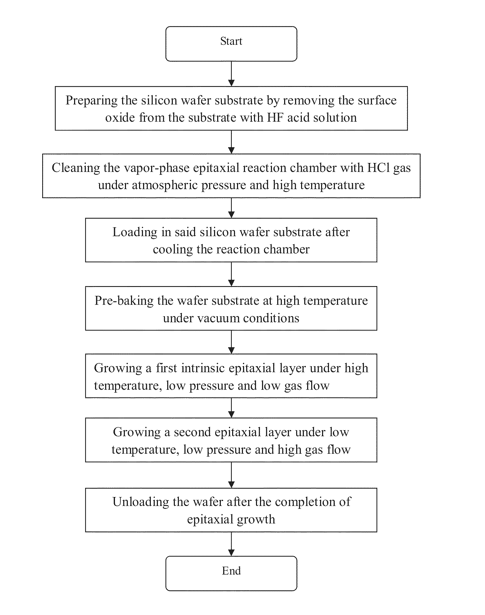
[0049]Please refer to FIG. 3. The method of epitaxial growth effectively preventing auto-doping effect of this embodiment comprises the following steps:

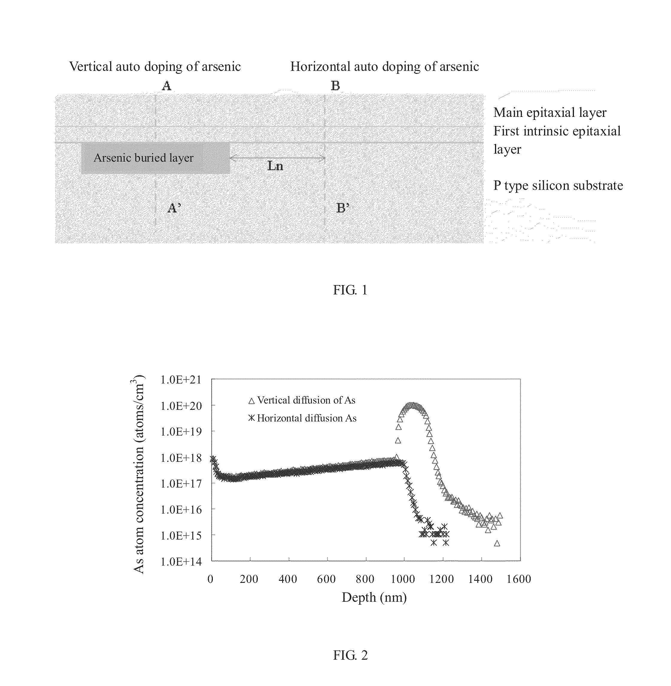
[0050]Firstly, form a silicon wafer substrate having heavily-doped buried layer region by As ion implantation, wherein the depth of said buried layer is 0.4 μm and the heavy doping concentration of said buried layer is 8E19 atoms / cm3.

[0051]Next, HF acid solution is used to remove the surface oxide from said silicon wafer substrate.

[0052]Next, before said silicon wafer substrate is loaded in the reaction chamber, introduce HCl gas into the reaction chamber to clean the reaction chamber under atmospheric pressure and high temperature (as the temperature graph shown in FIG. 4) so as to remove dopant atoms and other impurities absorbed on the inner wall of the reaction chamber, wherein preferred conditions are a temperature of 1190° C., a HCl flow of about 20 sccm, a carrier gas of N2 or H2, and a duration of 30 seconds.

[0053]Next, cool ...

embodiment 2

[0059]The method of epitaxial growth effectively preventing auto-doping effect of this embodiment comprises the following steps:

[0060]Step 1: form a silicon wafer substrate having heavily-doped buried layer by solid thermal diffusion of heavily As-doped silicon glass, wherein said buried layer has a depth of 0.5 microns and the heavy doping concentration of said buried layer is 3E19 atoms / cm3.

[0061]Step 2: remove the surface oxide from the silicon wafer substrate with HF acid solution.

[0062]Step 3: before said silicon wafer substrate is loaded in the reaction chamber, introduce HCl gas into the reaction chamber to clean the reaction chamber under atmospheric pressure and high temperature so as to remove dopant atoms and other impurities absorbed on the inner wall of the reaction chamber, wherein a typical temperature is 1190° C., a HCl flow is about 20 sccm, a carrier gas is N2 or H2, and a duration is 30 seconds.

[0063]Step 4: cool the reaction chamber to a low temperature (e.g., of...

embodiment 3

[0068]The method of epitaxial growth effectively preventing auto-doping effect of this embodiment comprises the following steps:

[0069]Firstly, form a silicon wafer substrate having heavily-doped buried layer by As ion implantation or by solid thermal diffusion of heavily As-doped silicon glass.

[0070]Next, remove the surface oxide from the silicon wafer substrate with HF acid solution.

[0071]Next, before said silicon wafer substrate is loaded in the reaction chamber, introduce HCl gas into the reaction chamber to remove, under atmospheric pressure and high temperature, dopant atoms and other impurities absorbed on the inner wall of the reaction chamber, wherein a typical temperature is 1190° C., a HCl flow is about 20 sccm, a carrier gas is N2 or H2, and a duration is 30 seconds.

[0072]Next, cool the reaction chamber to a low temperature (e.g., of about 850° C.) before load in said silicon wafer substrate.

[0073]Next, under vacuum conditions, pre-bake said silicon wafer substrate under ...


PUM

PropertyMeasurementUnit
temperatureaaaaaaaaaa
pressureaaaaaaaaaa
thicknessaaaaaaaaaa

Abstract

This invention relates to a method of epitaxial growth effectively preventing auto-doping effect. This method starts with the removal of impurities from the semiconductor substrate having heavily-doped buried layer region and from the inner wall of reaction chamber to be used. Then the semiconductor substrate is loaded in the cleaned reaction chamber to be pre-baked under vacuum conditions so as to remove moisture and oxide from the surface of said semiconductor substrate before the extraction of the dopant atoms desorbed from the surface of the semiconductor substrate. Next, under high temperature and low gas flow conditions, a first intrinsic epitaxial layer is formed on the surface of said semiconductor substrate where the dopant atoms have been extracted out. Following this, under low temperature and high gas flow conditions, a second epitaxial layer of required thickness is formed on the structural surface of the grown intrinsic epitaxial layer. Last, silicon wafer is unloaded after cooling. This method can prevent auto-doping effect during the epitaxial growth on semiconductor substrate and thus ensure the performance and enhance the reliability of the devices in peripheral circuit region.

Description

FIELD OF THE INVENTION[0001]The present invention relates to a semiconductor field, and more particularly to a method for preventing auto-doping effect on substrate having heavily-doped region during epitaxial growth.BACKGROUND OF THE INVENTION[0002]Epitaxial technology where heavily arsenic (As)-doped semiconductor acts as substrate has been increasingly widely used in device fabrication, and especially in diode, triode, VDMOS, varactor diode, IGBT and etc. With the miniaturization and the increase of integration level of devices, the consistency of epitaxial wafer having heavily As-doped silicon substrate and the transition region width of epitaxial layer are crucial for the performance and reliability of devices.[0003]During chemical vapor epitaxy, the impurity of As is unavoidable between the epitaxial layer and the heavily-doped region of substrate and between the epitaxial layer and the undoped region of substrate. Take the example of the growth of intrinsic epitaxial layer on...

Claims


Application Information

Patent Timeline
Patent Type & Authority Applications(United States)
IPC IPC(8): C30B25/18C30B23/02
CPCC30B25/02C30B29/06C30B23/025C30B25/186H01L21/02661H01L21/02532H01L21/02576H01L21/0262H01L21/02381
Inventor ZHANG, CHAOSONG, ZHITANGWAN, XUDONGLIU, BOWU, GUANPINGZHANG, TINGYANG, ZUOYA
Owner SHANGHAI INST OF MICROSYSTEM & INFORMATION TECH CHINESE ACAD OF SCI
Why Eureka
Try Eureka