Control scheme for 3D memory IC

Active Publication Date: 2013-06-13
NATIONAL TSING HUA UNIVERSITY
View PDF8 Cites 42 Cited by
  • Summary
  • Abstract
  • Description
  • Claims
  • Application Information

AI Technical Summary

Benefits of technology

[0010]An aspect of the present invention is to provide a 3D memory IC Semi-Master Slave scheme. Utilizing the design of self-timing control, based on the timing shift (offset) caused by the variation of the process, it can achieve self-timing of each chip layer of the

Problems solved by technology

However, the timing of its internal circuitry may critically affect the speed and efficiency of the SRAM.
For example, the bit line pre-charge interval comprises an appreciable portion of the read/write cycle time, and sense amplifier usage contributes significantly to the overall power consumption of the SRAM.
This potentially increases the overall operating speed of the memory device.
How

Method used


Image

  • Control scheme for 3D memory IC
  • Control scheme for 3D memory IC
  • Control scheme for 3D memory IC

Examples


Embodiment Construction

[0034]Some preferred embodiments of the present invention will now be described in greater detail. However, it should be recognized that the preferred embodiments of the present invention are provided for illustration rather than limiting the present invention. In addition, the present invention can be practiced in a wide range of other embodiments besides those explicitly described, and the scope of the present invention is not expressly limited except as specified in the accompanying claims.

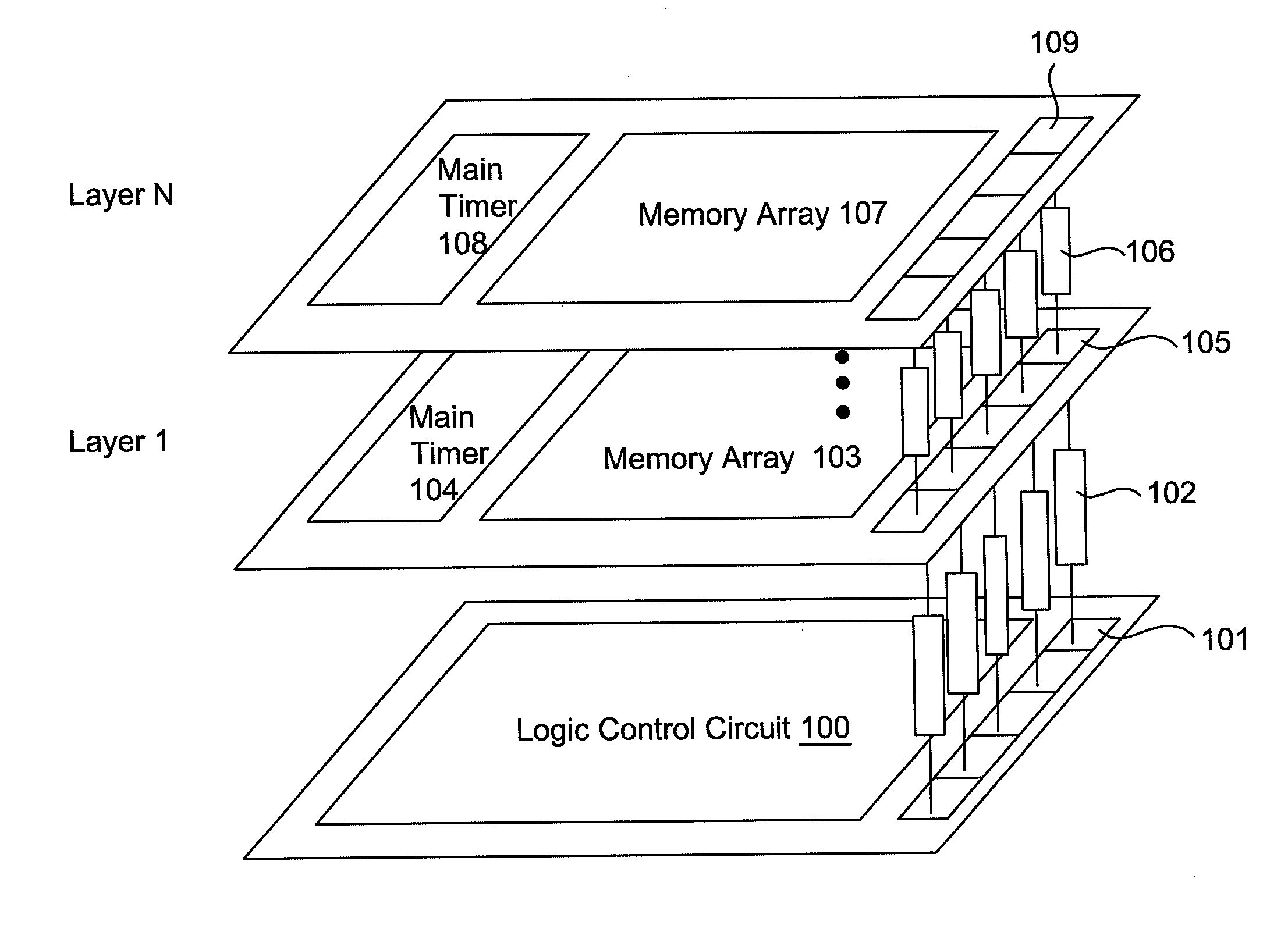
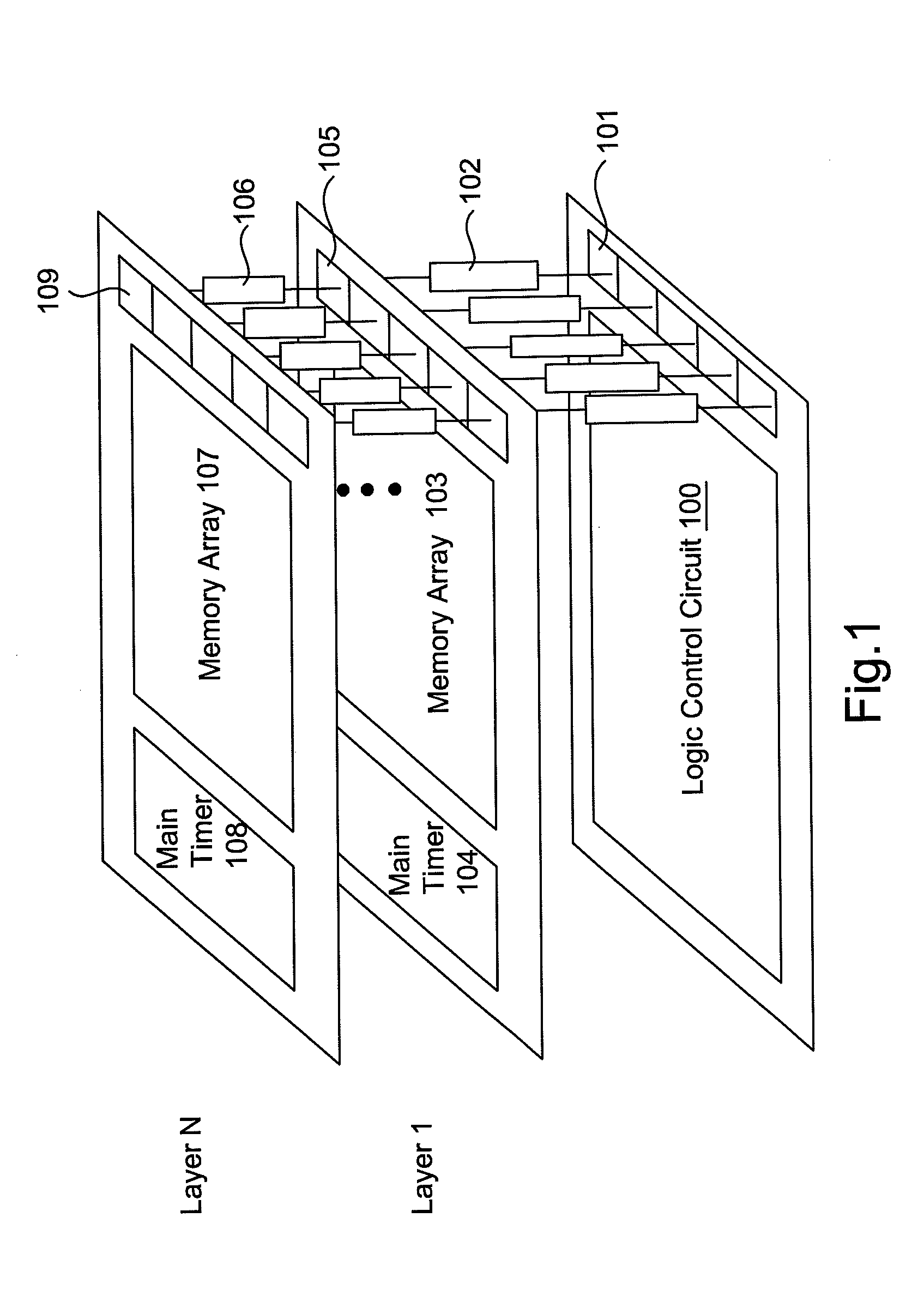
[0035]The present invention generally relates to a control scheme and a circuit mechanism capable of leakage current reduction for 3D memory IC which can be introduced to a 3D-SRAM. The present invention provides a Semi Master Slave (SMS) scheme and a Self-timed Differential-TSV signal transfer (STDT) scheme to 1). provide a constant-load logic-SRAM interface across various layer configurations; 2). suppress TSV-induced power and speed overheads; 3). tolerate die-to-die variation; and 4). enabl...


PUM


Abstract

The present invention discloses a control scheme for 3D memory IC that includes a master chip and at least one slave chip. The master chip includes a main memory core, a first local timer, an I/O buffer, a first pad and a second pad. The at least one slave chip is stacked with the master chip. Each of the slave chip includes a slave memory core, a second local timer and a third pad. A first TSV is coupled to the first pad and the third pad. A logic control circuit layer includes a logic control circuit and a fourth pad, and the logic control circuit is coupled to the fourth pad. A second TSV is coupled to the second pad and the fourth pad.

Description

TECHNICAL FIELD[0001]The present invention generally relates to a 3D stacked chip device, and especially relates to a control scheme and a circuit mechanism capable of leakage current reduction for 3D memory IC.BACKGROUND[0002]Recently, portable electronic equipment such as mobile telephones and non-volatile semiconductor memory media such as IC memory cards have been downsized, and there have been increasing demands for reducing the number of parts used in the equipment and media and downsizing thereof. Therefore, in the semiconductor industry, packaging technologies for integrated circuits (ICs) have been advancing to meet requirements for miniaturization and mounting reliability. For example, the requirement for miniaturization results in acceleration of technological development for a package having a similar size in relation to a semiconductor chip. Further, the requirement for mounting reliability places importance on packaging technologies that are capable of enhancing effici...

Claims


Application Information

Patent Timeline
IPC IPC(8): G11C5/06
CPCG11C8/08G11C11/417G11C29/023G11C29/028G11C2029/2602G11C29/26G11C2029/1202G11C2029/1206G11C29/04
Inventor CHANG, MENG-FANWU, WEI-CHENGHUANG, TSUNG-HSIENCHEN, CHIEN-YUAN
Owner NATIONAL TSING HUA UNIVERSITY
Why Eureka
Try Eureka