Memory device

a memory device and memory technology, applied in semiconductor devices, digital storage, instruments, etc., can solve the problems of small difference between electric charge amounts corresponding to different digital values, difficulty in maintaining data accuracy, and reducing capacitance values, so as to achieve high memory capacity, reduce errors, and maintain data retention. the effect of tim

Active Publication Date: 2013-06-13
SEMICON ENERGY LAB CO LTD
View PDF5 Cites 54 Cited by
  • Summary
  • Abstract
  • Description
  • Claims
  • Application Information

AI Technical Summary

Benefits of technology

[0027]According to one aspect of the disclosed invention, a memory device can have a sufficient data retention period and a higher memory capacity per unit area. According to another aspect of the disclosed invention, a ...

Problems solved by technology

However, a reduction in the area of the capacitor causes a decrease in the capacitance value, which results in a small difference between the amounts of electric charge corresponding to different digital values.
Thus, if the va...

Method used


Image

  • Memory device
  • Memory device
  • Memory device

Examples


example

[0297]In this example, operation of a memory device described in the embodiment is described.

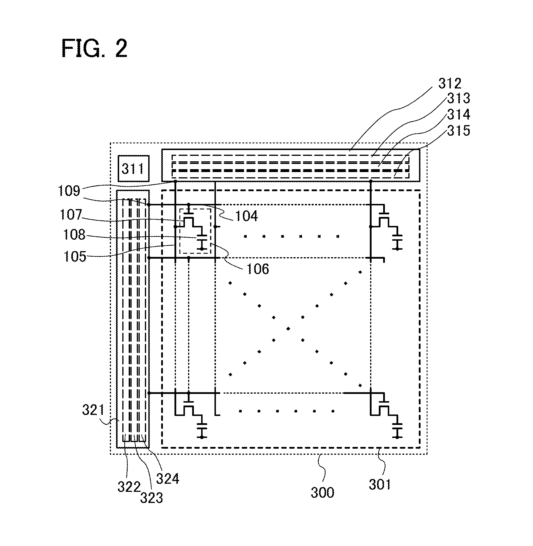
[0298]FIGS. 21A and 21B are circuit diagrams of a memory device used in this example. The memory device illustrated in FIG. 21A includes a memory cell array 401 (8 kb DOSRAM ARRAY), an input / output circuit 411, a bit line driver circuit 412 (also referred to as COLUMN DRIVER), and a word line driver circuit 421(also referred to as ROW DRIVER).

[0299]Note that in this specification, “DOSRAM” is an abbreviation for “dynamic oxide semiconductor random access memory” and is a memory device using the oxide semiconductor transistor described in the above embodiment as a selection transistor (a transistor as a switching element) of a memory cell. Extremely low off-state current of a selection transistor of a memory cell allows DOSRAM to retain data for a long time; accordingly, a reflesh cycle can be extremely long.

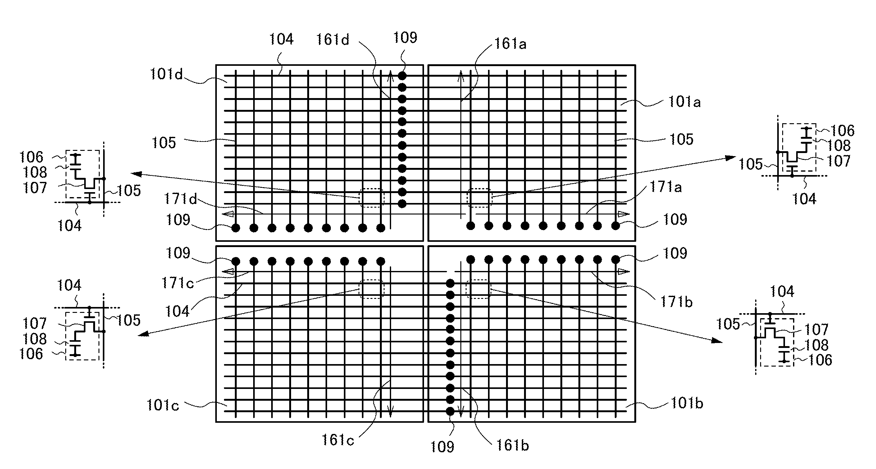
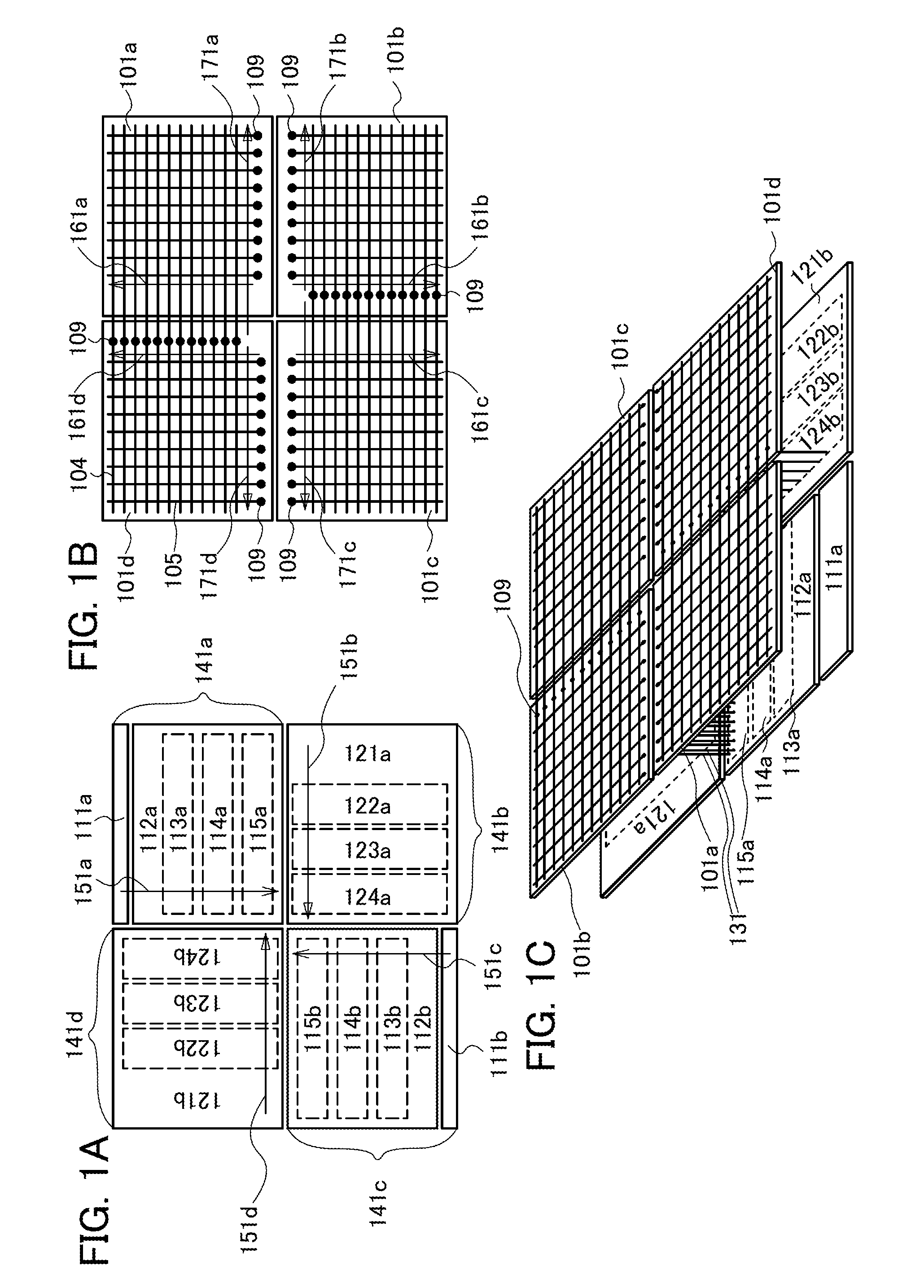
[0300]The memory cell array 401 includes a plurality of memory cells 406 (also referr...


PUM


Abstract

A memory device including first to fourth memory cell arrays and a driver circuit including a pair of bit line driver circuits and a pair of word line driver circuits is provided. The first to fourth memory cell arrays are overlap with the driver circuit. Each of the pair of bit line driver circuits and a plurality of bit lines are connected through connection points on an edge along the boundary between the first and second memory cell arrays or on an edge along the boundary between the third and fourth memory cell arrays. Each of the pair of word line driver circuits and a plurality of word lines are connected through second connection points on an edge along the boundary between the first and fourth memory cell arrays or on an edge along the boundary between the second and third memory cell arrays.

Description

BACKGROUND OF THE INVENTION[0001]1. Field of the Invention[0002]One aspect of the disclosed invention relates to memory devices and a manufacturing method thereof.[0003]2. Description of the Related Art[0004]A technique by which transistors are formed using semiconductor thin films formed over a substrate having an insulating surface has attracted attention. Transistors are used for display devices (typically, a liquid crystal television), memory devices where memory elements are arranged in matrix, and the like. Silicon is known as a material for a semiconductor thin film applicable to a transistor; however, an oxide semiconductor has attracted attention in recent years (see Patent Document 1).REFERENCE[0005][Patent Document 1] Japanese Published Patent Application No. 2011-109084SUMMARY OF THE INVENTION[0006]Examples of a semiconductor memory device (hereinafter also simply referred to as a memory device) include a DRAM and an SRAM, which are categorized as volatile memories; a ma...

Claims


Application Information

Patent Timeline
IPC IPC(8): G11C8/08G11C11/24
CPCG11C8/08G11C11/24G11C11/404H01L27/1225H01L27/0207H01L27/10882H01L27/10897G11C11/4097H10B12/48H10B12/50
Inventor ATSUMI, TOMOAKIOKUDA, TAKASHI
Owner SEMICON ENERGY LAB CO LTD
Why Eureka
Try Eureka