Method of Controlling Semiconductor Device Fabrication

a technology of semiconductor devices and metrology, applied in the direction of material strength analysis using repeated/pulsating forces, material strength analysis using sonic/ultrasonic/infrasonic waves, etc., can solve the problem of not being able to perform non-destructive stress measurements on thin sin films formed on product wafers, and achieve the effect of monitoring the effectiveness of any fabrication process step

Active Publication Date: 2013-06-13
METRYX
View PDF0 Cites 7 Cited by
  • Summary
  • Abstract
  • Description
  • Claims
  • Application Information

AI Technical Summary

Benefits of technology

The patent text describes a method for detecting problems in a semiconductor wafer fabrication process by measuring the mass of the wafers and comparing it to a characteristic mass change distribution. This method can provide useful information about the process even when there are only limited non-destructive measurements available. The measured mass change distribution can indicate changes in parameters such as thickness, layer uniformity, stoichiometry, stress, and refractive index. The method can also help identify problems with individual wafers by measuring the mass change distribution of each wafer and comparing it to the characteristic distribution. The method can be used in a statistical process control (SPC) system to monitor the effectiveness of the fabrication process and remedy any problems in a timely manner. The method can also be combined with other non-destructive metrology techniques to pick up anomalies or errors that may be undetected using other methods.

Problems solved by technology

For example, it is not possible to perform non-destructive measurements of stress on thin SiN films formed on product wafers.

Method used


Image

  • Method of Controlling Semiconductor Device Fabrication
  • Method of Controlling Semiconductor Device Fabrication
  • Method of Controlling Semiconductor Device Fabrication

Examples


Embodiment Construction

Further Options and Preferences

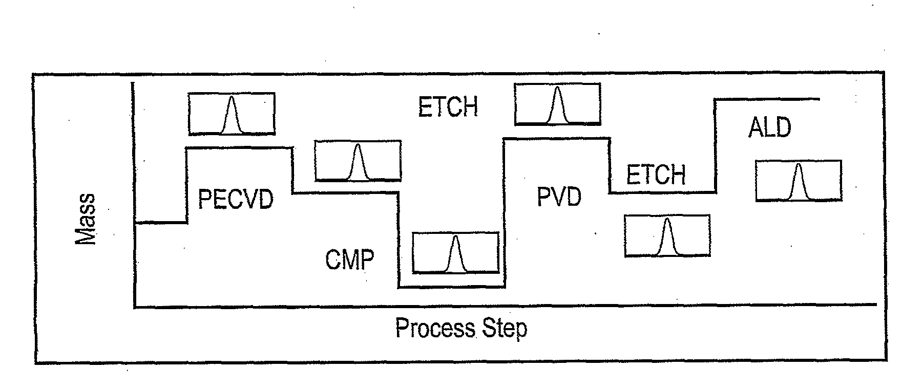
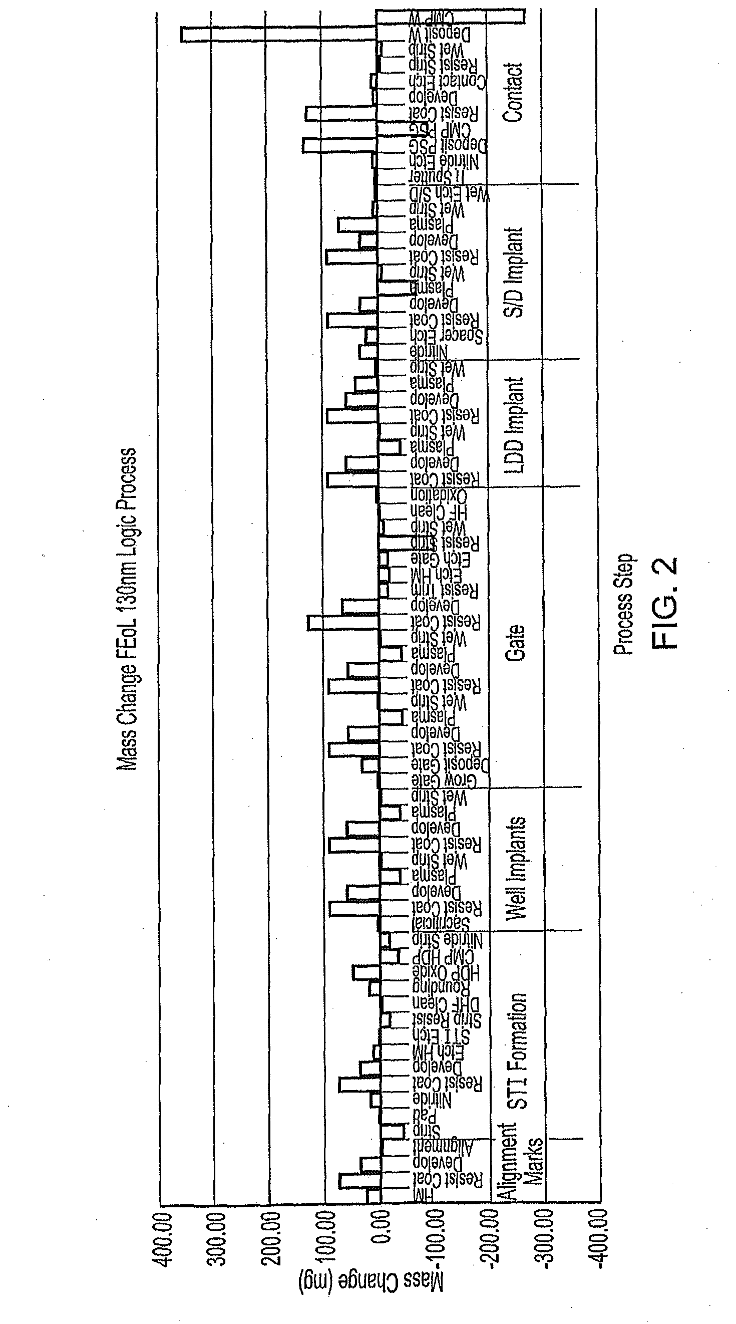
[0060]FIG. 1 illustrates schematically the idea that every step in a semiconductor fabrication process involves a change in mass. Moreover, each process will have a characteristic mass change with its own distribution. The chart in FIG. 1 shows how the mass (on the y-axis, not to scale) of a semiconductor wafer may change according to the type of fabrication process it experiences. Thus, a plasma enhanced chemical vapour deposition (PECVD) increases mass, chemical mechanical polishing (CMP) and etch processing decrease mass, and physical vapour deposition (PVD) and atomic layer deposition (ALD) increase mass. Each of the mass changes has a different magnitude. An accurate mass measurement may be able to detect these changes to generate a measured mass change distribution for a plurality of semiconductor wafers which are treated. By comparing individual mass change measurements or the measured mass change distribution to a characteristic mass change dis...


PUM


Abstract

A semiconductor wafer fabrication metrology method in which process steps are characterised by a change in wafer mass, whereby during fabrication mass is used as a measurable parameter to implement statistical process control on the one or more of process steps. In one aspect, the shape of a measured mass distribution is compared with the shape of a predetermined characteristic mass distribution to monitor the process. An determined empirical relationship between a control variable of the process and the characteristic mass change may enable differences between the measured mass distribution and characteristic mass distribution to provide information about the control variable. In another aspect, the relative position of an individual measured wafer mass change in a current distribution provides information about individual wafer problems independently from general process problems.

Description

CROSS REFERENCE TO RELATED APPLICATIONS[0001]This application is a continuation of application Ser. No. 12 / 811,855, filed Jul. 7, 2010, which is the National Stage of International Application No. PCT / GB09 / 00043, filed Jan. 7, 2009; which claims priority benefit of UK Application No. 0800227.1 filed Jan. 7, 2008 (which are hereby incorporated by reference).FIELD OF THE INVENTION[0002]This invention relates to semiconductor wafer metrology.BACKGROUND TO THE INVENTION[0003]Microelectronic devices are fabricated on semiconductor wafers using a variety of techniques, e.g. including deposition techniques (CVD, PECVD, PVD, etc.) and removal techniques (e.g. chemical etching, CMP, etc.). Semiconductor e.g. silicon wafers may be further treated in ways that alter their mass e.g. by cleaning, ion implantation, lithography and the like.[0004]Depending on the device being manufactured, each wafer may be passed sequentially through hundreds of different processing steps to build up and / or to re...

Claims


Application Information

Patent Timeline
Patent Type & Authority Applications(United States)
IPC IPC(8): H01L21/66
CPCG05B15/02G05B23/024H01L22/12H01L2924/0002H01L2924/00
Inventor KIERMASZ, ADRIAN
Owner METRYX
Why Eureka
Try Eureka