Method for manufacturing organic semiconductor thin film and monocryastalline organic semiconductor thin film

Active Publication Date: 2013-06-13
NAT INST OF ADVANCED IND SCI & TECH
View PDF7 Cites 5 Cited by
  • Summary
  • Abstract
  • Description
  • Claims
  • Application Information

AI Technical Summary

Benefits of technology

This patent describes a method for producing high-quality organic semiconductor layers using a printing process. The method avoids the formation of aggregates on the surface of the layers, resulting in more uniform quality and film thickness. This allows for the construction of organic semiconductor devices with superior properties. The method is also suitable for mass production using inexpensive roll-to-roll operation. Additionally, the patent describes a method for producing monocrystalline organic semiconductor layers, which results in devices with improved performance without the presence of grain boundaries.

Problems solved by technology

In contrast, an organic semiconductor of low molecular system obtaining higher device property compared with high molecular system is difficult to form a uniform semiconductor layer due to a low viscosity of a solution and a highly crystalline property possessed by the low molecular organic semiconductor.
However, in this method, since the deposition of the organic semiconductor proceeds with generation of convection inside the droplet after dropping the ink, the deposition of the material is concentrated on the peripheral portion of the droplet where the solvent is mainly evaporated.
However, the method is not sufficient in terms that the property deteriorates because the polymer unrelated the conductivity is mixed with the low molecular organic semiconductor and of controllability, uniformity, etc. of the entire film formation obtained by dropping.
However, the above methods are limited in case in which in the molecule compound consisting of two kinds of molecules, a great difference in solubility between the material molecules and the compound can be utilized.
Since low molecular organic semiconductors obtaining high device property is mostly organic materials consisting of single component organic molecules, the above-mentioned ink jet printing method cannot be applied to it.
However, the above methods are insufficient in terms of manufacturing a monocrystalline organic semiconductor thin film with good controllability in an industrially mass producible level.
Moreover, regarding the application of a printing technique, in particular, for effectively utilizing property of organic electronics, no effective methods applicable to the monocrystalline organic semiconductor device have been known.

Method used


Image

  • Method for manufacturing organic semiconductor thin film and monocryastalline organic semiconductor thin film
  • Method for manufacturing organic semiconductor thin film and monocryastalline organic semiconductor thin film
  • Method for manufacturing organic semiconductor thin film and monocryastalline organic semiconductor thin film

Examples


example 1

[0030]This example relates to manufacturing an organic semiconductor thin film. The example using 6,13-bistriisopropylsilylethynyl pentacene (hereinafter, abbreviated as “TIPS pentacene”) reported as a material forming an organic semiconductor layer to manufacture an organic thin film transistor is described in Example 1.

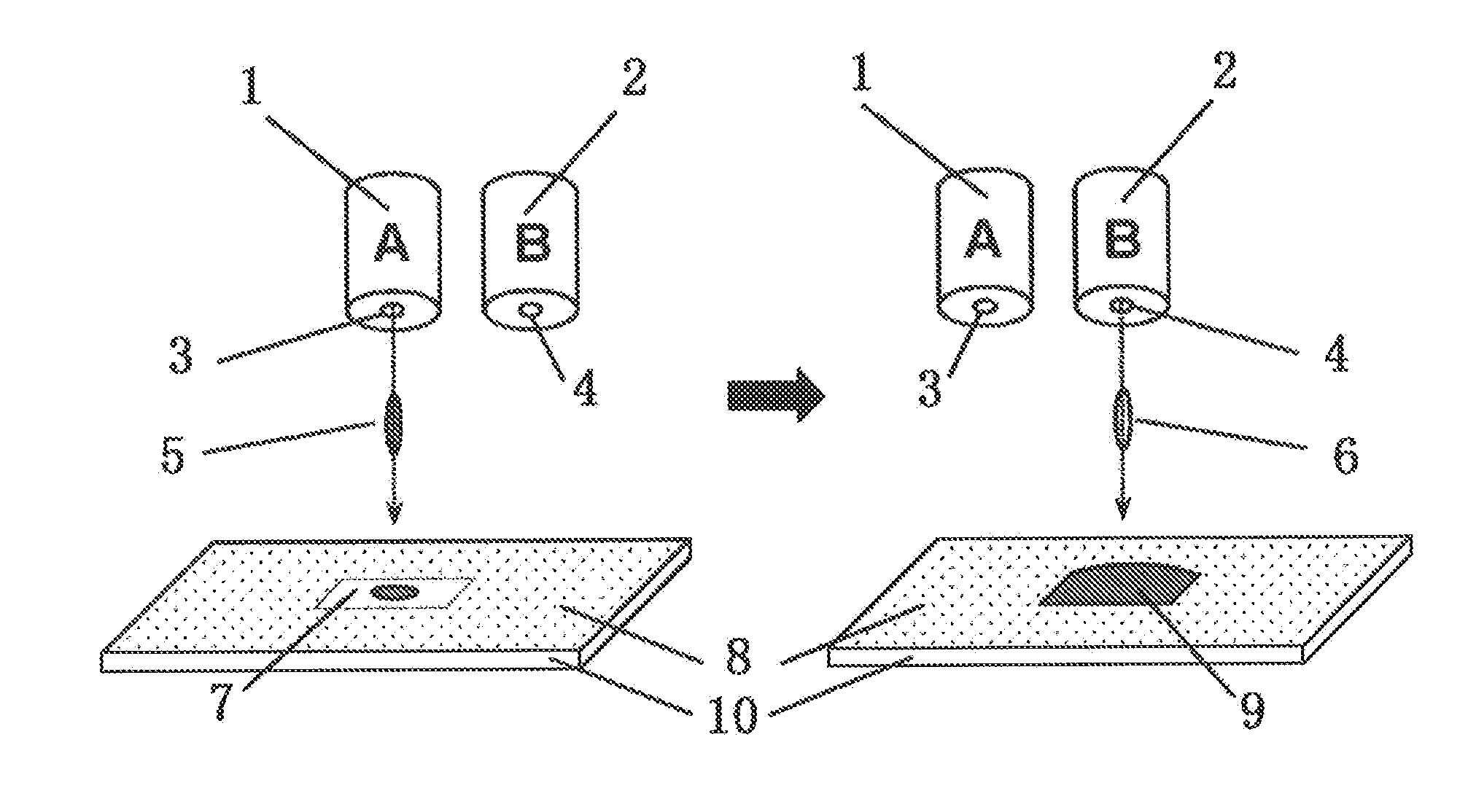
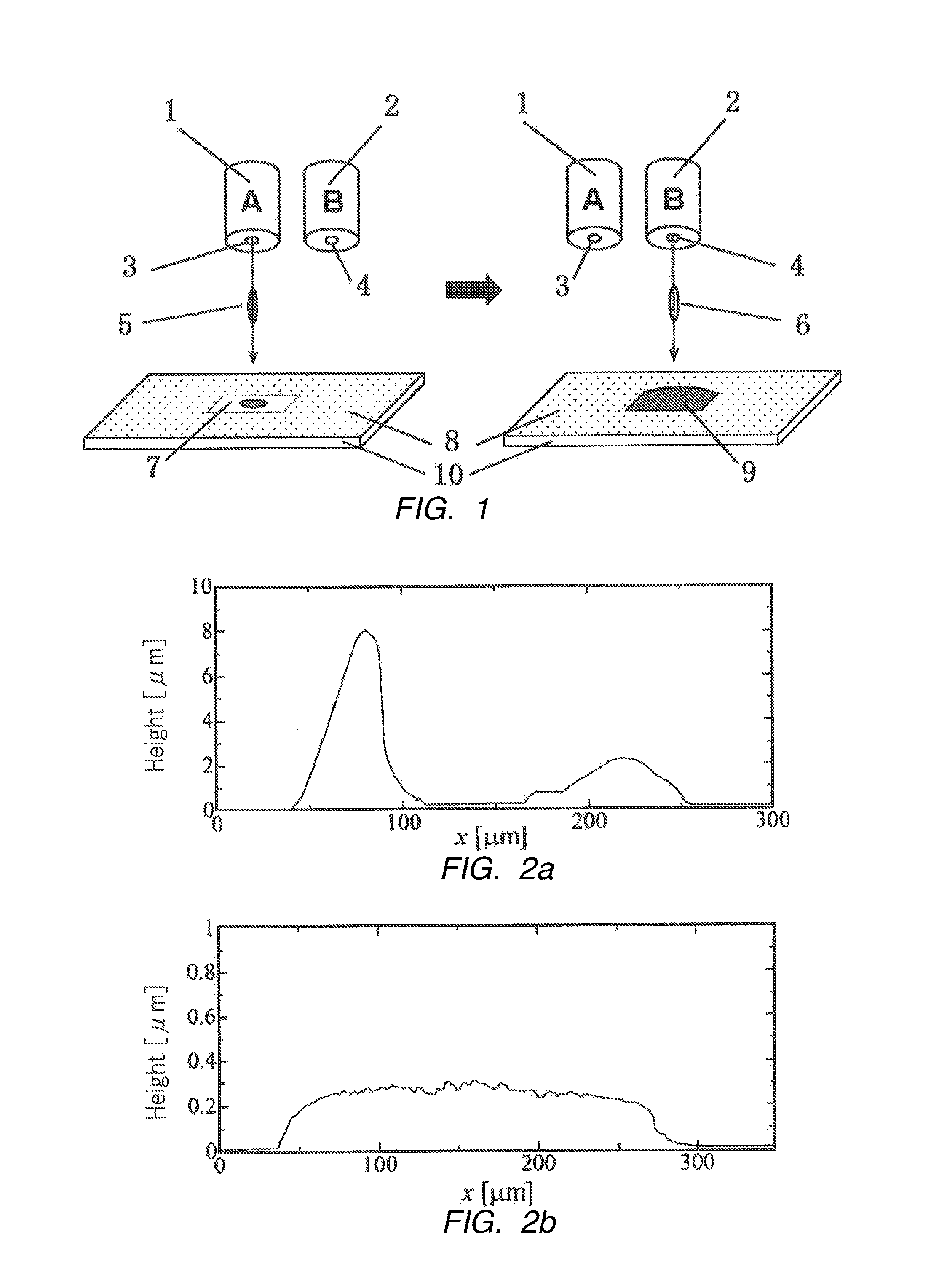
[0031]Chlorobenzene (CB) was used as a solvent for dissolving TIPS pentacene at a high concentration. N,N-dimethyl formamide (DMF) was prepared as a solvent for hardly dissolving TIPS pentacene. Thus, a TIPS pentacene thin film was manufactured by using an ink jet device with two ink jet heads capable of individually discharging.

[0032]Each of Materials, TIPS pentacene, CB and DMF is obtainable at low costs. A Refined TIPS pentacene was applied by re-crystallization method.

[0033]First, 36.3 mmol / l of TIPS pentacene solution of which concentration is used as an ink was prepared by dissolving TIPS pentacene (31 mg) (48.5 μmol: molecular weight 639) in 1.3 ml of chlorob...

example 2

[0049]This example relates to manufacturing a monocrystalline organic semiconductor thin film. In this case, C8-BTBT with high crystalline property was used as an organic material constituting an organic semiconductor layer. An organic semiconductor layer was formed using an ink formed by dissolving dissolving a high concentration of the above organic semiconductor and an ink of an organic solvent hardly dissolving the organic semiconductor by the double shot-ink jet printing method explained in example 1.

[0050]A region stored an ink dropped on a substrate by the ink jet printing method was defined by patterning by both hydrophilic (lipophilic) and hydrophobic treatments on the substrate surface. The region is surface-treated so that it has preliminarily designed shape to relatively quickly evaporate the solvent at a certain portion and to generate a seed crystal to form a monocrystalline organic semiconductor thin film.

[0051]The present invention will explain based upon the followi...


PUM


Abstract

The first object of the present invention is to provide a method for manufacturing a uniform organic semiconductor thin film consisting of single organic molecule with extremely few pinholes and of which both quality and thickness are uniform when the organic semiconductor thin film is manufactured by printing process. The second object of the present invention is to manufacture a monocrystalline organic semiconductor of which almost the entire region consists of a single monocrystal, by printing process.The uniform organic semiconductor thin film is manufactured by steps of: preparing a first ink obtained by dissolving a high concentration of the organic semiconductor in an organic solvent with high affinity for the organic semiconductor, and a second ink consisting of an organic solvent having a low affinity for the organic semiconductor; mixing the first and second inks on a substrate by simultaneously or alternately discharging the first and second inks from each ink head. Furthermore, a shape on which a seed crystal is generated with highly efficiency in one portion of a region storing the ink and a monocrystal is grown over the almost entire region storing the ink from the shape as a starting point.

Description

CROSS-REFERENCE TO RELATED APPLICATION[0001]The present application claims priority from International Patent Application Serial No. PCT / JP2011 / 068294 filed Aug. 10, 2011; Japanese Patent Applications Nos. JP2010-182945 filed on Aug. 18, 2010 and No. 2010-189315 filed on Aug. 26 2010, the contents of which are hereby incorporated by reference into this application.TECHNICAL FIELD OF THE INVENTION[0002]The present invention relates to method for manufacturing an organic semiconductor thin film and a monocrystalline organic semiconductor thin film.BACKGROUND OF THE INVENTION[0003]Organic electronics using organic semiconductors of both high molecular and low molecular have noticed as a major next-generation technology for manufacturing flat panel displays and electronic paper. Recently, it has been highly progressed that an organic electric field light emission diode having been manufactured as a commercial reality and researches and developments for an organic semiconductor thin film...

Claims


Application Information

Patent Timeline
IPC IPC(8): H01L51/00
CPCH01L51/0005H01L51/0094C09D11/52H01L51/0007C09D11/322H01L51/0002H10K71/15H10K71/135H10K85/40H10K71/10
Inventor HASEGAWA, TATSUOMINEMAWARI, HIROMIYAMADA, TOSHIKAZUMATSUI, HIROYUKI
Owner NAT INST OF ADVANCED IND SCI & TECH
Why Eureka
Try Eureka