
Low contact resistance organic thin film transistors

a thin film transistor, low contact resistance technology, applied in the direction of organic conductors, non-metal conductors, conductors, etc., can solve the problems of difficult to obtain repeatable results from solution processed films, film roughness, and limit the performance of these materials in devices, so as to reduce contact resistance

Active Publication Date: 2013-06-13
CAMBRIDGE DISPLAY TECH LTD
View PDF9 Cites 9 Cited by
  • Summary
  • Abstract
  • Description
  • Claims
  • Application Information

AI Technical Summary

Benefits of technology

The patent text describes a method for reducing contact resistance in organic thin film transistors by using a solvent selected from the group ofC1-4 alkoxybenzenes and C1-4 alkyl substituted C1-4 alkoxybenzenes to prepare the semiconductor blend formulation for depositing as a semiconductor layer. The use of this solvent results in a significant reduction of contact resistance compared to using xylene, which can contribute a significant proportion to the total channel resistance in the device. This is important for minimizing the contact resistance in organic thin film transistors with short channel lengths and produces devices with higher mobility. The method is simple and cost-effective.

Problems solved by technology

Although small molecule semiconductor materials can exhibit high mobilities due to their highly crystalline texture (particularly as thermally evaporated thin films) it can often be difficult to obtain repeatable results from solution processed films due to their poor film forming properties.
Issues with material reticulation from and adhesion to substrates, film roughness and film thickness variations can limit the performance of these materials in devices.
Film roughness can be a further problem for top-gate organic thin film transistor devices, as the accumulation layer is formed at the uppermost surface of the semiconductor layer.
nisole. However, there is no disclosure or suggestion in WO 2005 / 055248 that its use would reduce contact res
However, there is no correlation between the disclosed properties and contact resistance.
No research has been conducted into the solvent selection to reduce contact resistance in devices incorporating semiconductor blends.
A high contact resistance has the effect of a much lower current level being extracted from the device due to the lower bias applied across the channel region, and hence lower device mobility.
For small molecule materials such as benzothiophene derivatives and pentacene derivatives a low solubility is found (0.4% w / v limit) and a poor film quality is also found.
In some instances, these methods alone are not sufficient to minimise the contact resistance.

Method used


Image

  • Low contact resistance organic thin film transistors
  • Low contact resistance organic thin film transistors
  • Low contact resistance organic thin film transistors

Examples


example 1

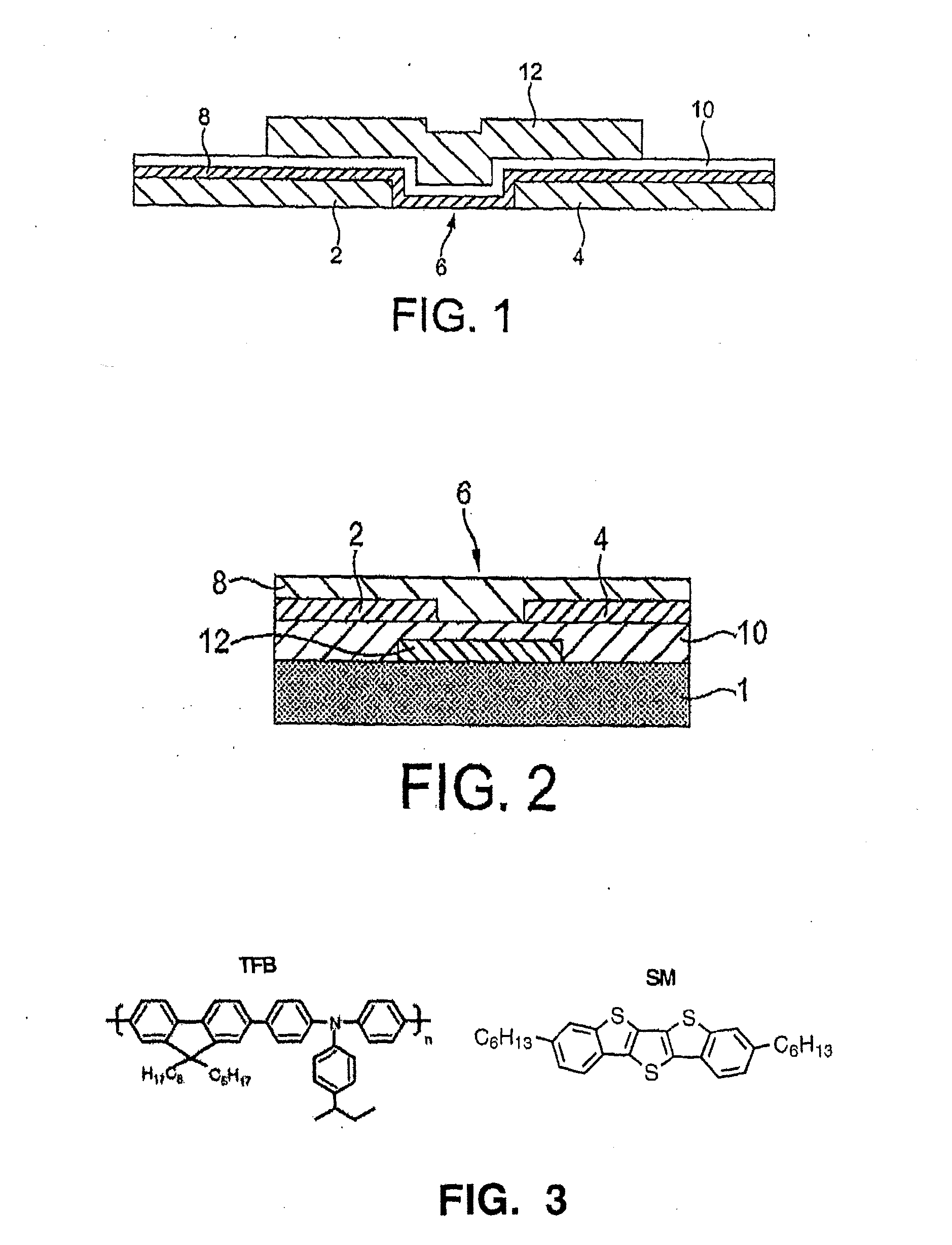
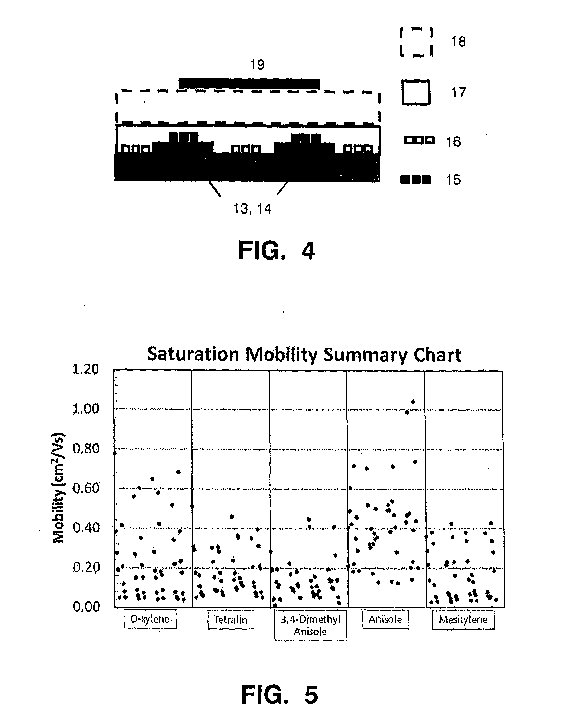
[0207]In this first example, data were obtained from devices prepared as described in the above preparative example with semiconductor layers deposited from anisole, and these were compared with data obtained from reference examples of devices with films cast from other solvents, namely o-xylene, tetralin, dimethylanisole and mesitylene. The saturation mobility of the resulting devices was measured and is shown in FIG. 5.

[0208]From FIG. 5, the mobility ranges were measured for 5 to 100 μm devices, and these are set out in Table 1 below.

TABLE 1DimethylO-xyleneTetralinanisoleAnisoleMesityleneMobility range0.0390.0519.4 × 1030.1240.025(cm2 / Vs)to 0.778to 0.510to 0.448to 1.040to 0.428For 5 to 100μm devices

[0209]The range in mobilities arises from the range of channel lengths used in the test cells (5 to 100 μm). Devices with the shortest channel lengths were found to exhibit lower mobilities (contact resistance is the more dominant component compared to the total channel resistance) and ...

example 2

[0211]A reduced contact resistance is only part of the reason for realising an improved device performance when using the solvents of the invention such as anisole as the organic semiconductor solvent in place of xylene or another conventional solvent. In addition to a lower absolute contact resistance, the proportion of contact resistance to the total channel resistance was also found to be lower for devices using the solvents of the invention such as anisole. Table 2 below highlights the average values of contact and channel resistances for a series of devices with organic semiconductor layers deposited from xylene or anisole. The devices were produced by depositing an SM:TFB organic blend with a mass ratio of 70:30 respectively from a solution thereof in the tested solvents. Values were calculated for a gate bias of −40 V, and normalised to the channel width (all devices have a channel width of 2 mm).

[0212]The total channel resistance shown in Table 2 below is defined as the sum ...

example 3

[0215]In this example, further solvents were tested and also found to have superior properties in reducing contact resistance. Devices were prepared as in the preparative example using a solution of a 30:70 mix of polymer component TFB and small molecule component SM in the solvents 2-methylanisole and 4-methylanisole as the organic semiconducting layer. Comparative devices were also prepared using anisole (another according to the invention) and o-xylene as solvents, as in Example 1. The average saturation mobility of the devices was measured and is shown in FIG. 7 together with the average contact resistance for each of the devices.

[0216]The results clearly show that the devices prepared using 2-methylanisole and 4-methylanisole as the solvent in depositing the organic semiconductor blend have significantly lower contact resistance values and higher average saturation regime mobilities than that obtained from inks produced in o-xylene. Due to the lower contact resistance for these...


PUM

PropertyMeasurementUnit
Fractionaaaaaaaaaa
Fractionaaaaaaaaaa
Lengthaaaaaaaaaa

Abstract

The invention provides the use of a solvent selected from the group consisting of alkoxybenzenes and alkyl substituted alkoxybenzenes in reducing the contact resistance in an organic thin film transistor comprising a semiconductor layer comprising a blend of a small molecule semiconductor material and a polymer material that is deposited from a solution of said small molecule semiconductor material and said polymer material in said solvent and novel semiconductor blend formulations that are of particular use in preparing organic thin film transistors. Said solvents yield devices with lower absolute contact resistance, lower absolute channel resistance, and lower proportion of contact resistance to the total channel resistance.

Description

[0001]The present invention relates to organic thin film transistors, and in particular to the reduction of contact resistance in said transistors, especially those with a short channel length.BACKGROUND OF THE INVENTION[0002]Transistors can be divided into two main types: bipolar junction transistors and field-effect transistors. Both types share a common structure comprising three electrodes with a semiconductive material disposed therebetween in a channel region. The three electrodes of a bipolar junction transistor are known as the emitter, collector and base, whereas in a field-effect transistor the three electrodes are known as the source, drain and gate. Bipolar junction transistors may be described as current-operated devices as the current between the emitter and collector is controlled by the current flowing between the base and emitter. In contrast, field-effect transistors may be described as voltage-operated devices as the current flowing between source and drain is con...

Claims


Application Information

Patent Timeline
IPC IPC(8): H01L51/00
CPCH01L51/0007H01L51/0035H01L51/004H01L51/0043H01L51/0034H01L51/0541H01L51/0545H01L51/0003H01L51/0074H10K71/15H10K85/141H10K85/111H10K85/151H10K85/6576H10K10/464H10K10/466H10K10/488H10K10/00H10K85/10H10K71/12
Inventor NEWSOME, CHRISTOPHER
Owner CAMBRIDGE DISPLAY TECH LTD
Learn More