Method for suppressing kirkendall voids formation at the interface between solder and copper pad

a technology of kirkendall voids and copper pads, which is applied in the direction of welding/cutting media/materials, manufacturing tools, and soldering apparatus, etc., can solve the problems of mechanical/electrical degradation of solder joints

Inactive Publication Date: 2013-06-20
YUAN ZE UNIV
View PDF7 Cites 53 Cited by
  • Summary
  • Abstract
  • Description
  • Claims
  • Application Information

AI Technical Summary

Benefits of technology

[0007]An embodiment of the present invention, which is very beneficial to the mechanical reliability of the solder joints, is directed to a method for suppressing Kirkendall voids formation at the interface between a solder and a copper pad.
[0014]In view of the foregoing, in the present invention, a minor amount of palladium is doped into the solder before the solder is joined to the copper pad. The quantity of the Kirkendall voids formed at the interface between the copper pad and the Cu3Sn layer can be substantially reduced by minor addition of palladium, and the mechanical properties of the solder joints can be significantly enhanced due to the decrease of Kirkendall voids.

Problems solved by technology

The Kirkendall voids might propagate with the growth of Cu3Sn and provide a crack initiation site in the subsequent drop test, thereby causing a mechanical / electrical degradation of solder joints.
Therefore, to reduce the growth of Cu3Sn as well as that of Kirkendall voids has long been recognized as an important reliability issue in the microelectronic packaging.

Method used


Image

  • Method for suppressing kirkendall voids formation at the interface between solder and copper pad
  • Method for suppressing kirkendall voids formation at the interface between solder and copper pad
  • Method for suppressing kirkendall voids formation at the interface between solder and copper pad

Examples


Embodiment Construction

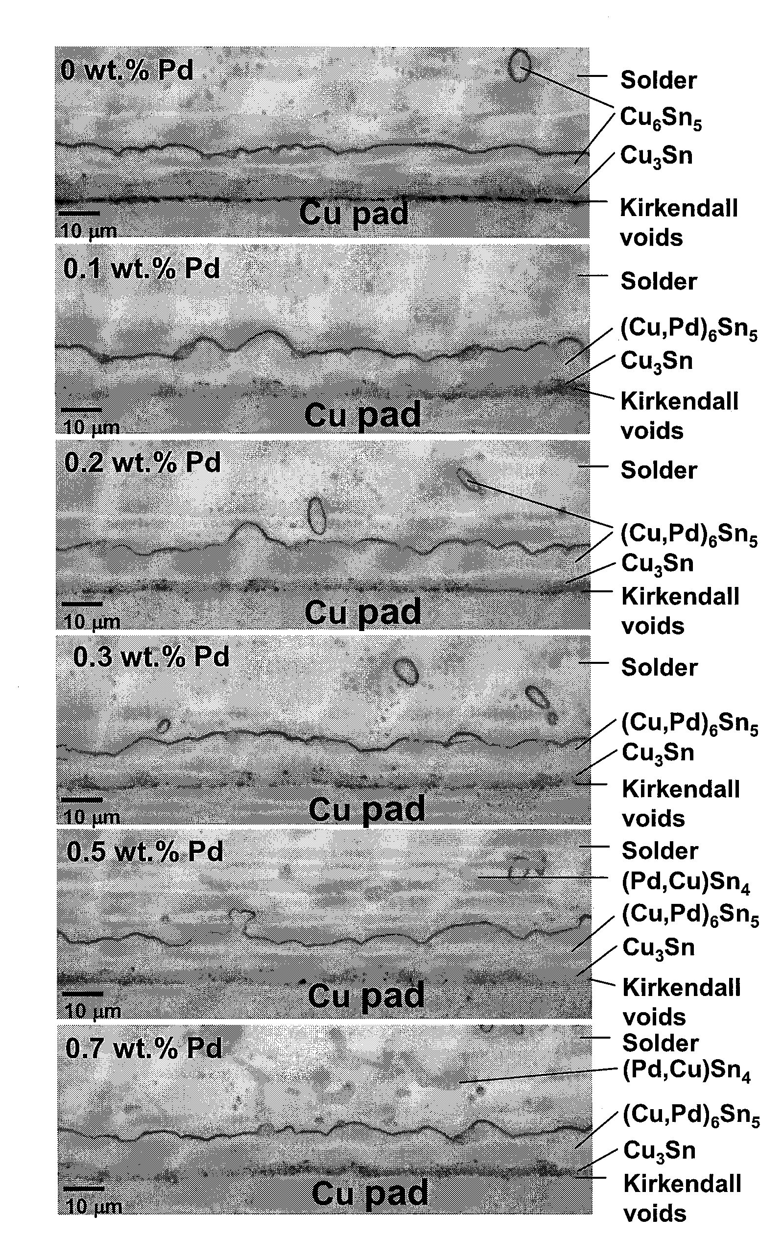
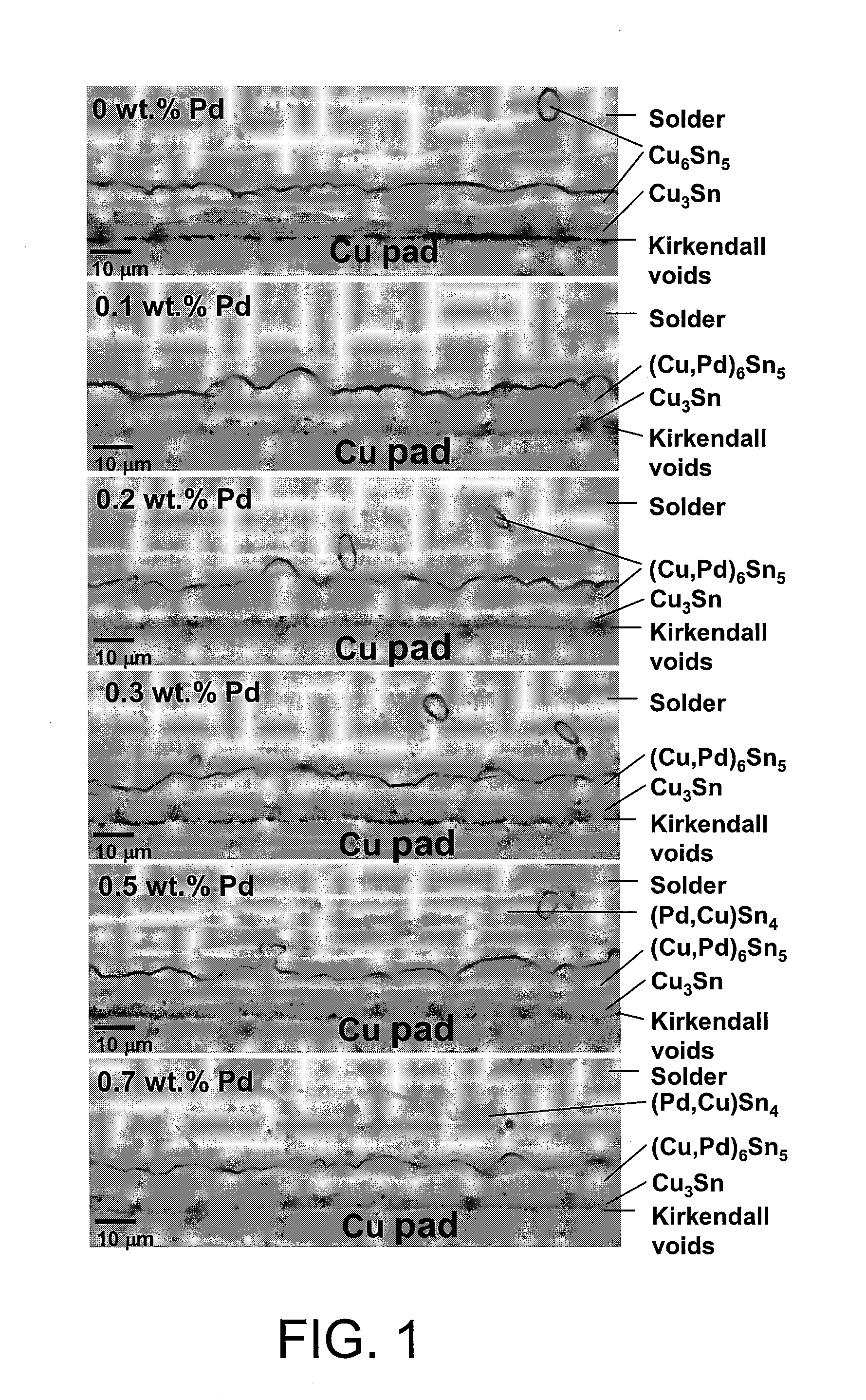
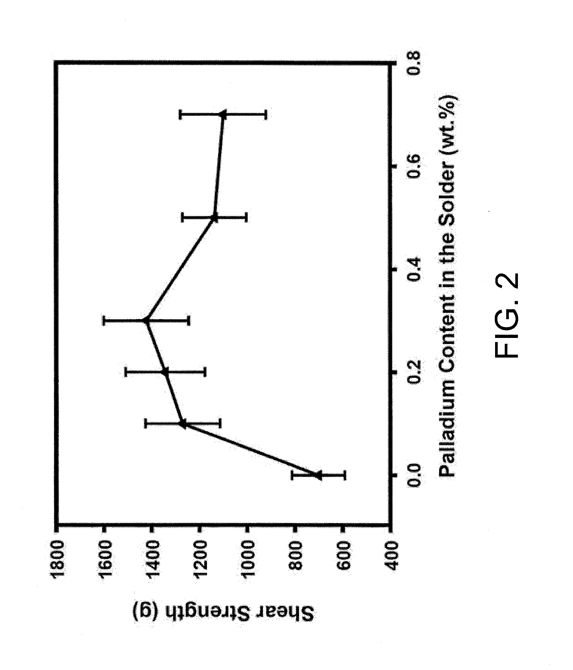
[0019]Several remedies have been proposed in the past few years for suppressing Kirkendall voids formation at the interface between a solder and a copper pad. The first method is to deposit an additional metal film over the copper pad as a diffusion barrier that is not allowable to be removed during soldering or subsequently solid-state aging. The second is to fine-tune the interfacial microstructures by doping a certain amount of element(s) into the solder or the copper pad before soldering.

[0020]In the first method, the interdiffusion between copper (copper pad) and tin atoms (solder) is prohibited by the diffusion barrier, thereby avoiding the formation of Cu-Sn IMCs and Kirkendall voids at the interface between the copper pad and the solder. The nickel-based metal, such as pure nickel (Ni), nickel-copper (Ni-Cu) alloy, nickel-vanadium (Ni-V) alloy, or nickel-phosphorus (Ni-P) alloy, is realized to be the diffusion barrier material of choice. However, the wettability between the ...


PUM

PropertyMeasurementUnit
diameteraaaaaaaaaa
temperatureaaaaaaaaaa
thicknessaaaaaaaaaa

Abstract

The embodiment of the present invention relates to a method for suppressing Kirkendall voids formation in a solder joint. A solder alloy doped with 0.1˜0.7 weight percent (wt. %) of palladium (Pd) is utilized. Before soldering, the solder alloy is disposed on a copper (Cu) pad, possibly treated with a surface finish. Subsequently, the solder alloy is joined with the Cu pad, so as to form the solder joint with a Cu / Cu3Sn / (Cu,Pd)6Sn5 / solder structure. The formation of Kirkendall voids at the Cu / Cu3Sn interface is greatly suppressed in the presence of Pd in the solder. As the amount of Pd doped is minimal, the properties and the processing conditions for soldering are not changed to a large extent, and the mechanical reliability of the solder joint is significantly improved. Therefore, the present invention is suitable for the microelectronic packaging applications.

Description

CROSS-REFERENCE TO RELATED APPLICATION[0001]This application claims the priority benefit of Taiwan application serial no. 100146221, filed on Dec. 14, 2011. The entirety of the above-mentioned patent application is hereby incorporated by reference herein and made a part of this specification.BACKGROUND OF THE INVENTION[0002]1. Field of the Invention[0003]The present invention relates to a method for enhancing the mechanical reliability of solder joints, and more particularly, to a method for suppressing Kirkendall voids formation at the interface between a solder and a copper pad.[0004]2. Description of Related Art[0005]Soldering is a metallization process, in which two individual components are joined by using a molten solder alloy. Solders used in the microelectronic packages are mostly tin-based alloys, such as tin-lead (Sn-Pb) alloy, tin-zinc (Sn-Zn) alloy, tin-bismuth (Sn-Bi) alloy, tin-indium (Sn-In) alloy, tin-antimony (Sn-Sb) alloy, tin-copper (Sn-Cu) alloy, tin-silver (Sn-A...

Claims


Application Information

Patent Timeline
Patent Type & Authority Applications(United States)
IPC IPC(8): B23K31/02B23K1/20
CPCB23K1/0016B23K1/203B23K35/0222B23K2201/42B23K35/302B23K35/34B23K2101/42
Inventor HO, CHENG-EN
Owner YUAN ZE UNIV
Why Eureka
Try Eureka