Apparatus And Method Of Measuring Roughness And Other Parameters Of A Structure

Active Publication Date: 2013-07-18
KLA TENCOR CORP
View PDF2 Cites 50 Cited by
  • Summary
  • Abstract
  • Description
  • Claims
  • Application Information

AI Technical Summary

Benefits of technology

[0018]In some embodiments, a beam profile reflectrometry (BPR) system is used to perform speckle metrology on a specimen under inspection in accordance with the exemplary methods presented herein. In some embodiments, beam profile reflectometers employ one or more laser based illumination sources that provide illumination with a high degree of spatial coherence. In some other embodiments, non-laser based illumin

Problems solved by technology

Primary disadvantages of SEM (a.k.a., CD-SEM) include limited viewing angles and a potentially destructive impact on structures under examination.
This is especially undesirable in resist metrology.
For the case of TEM, destructive testing of the sample is required in addition to the aforementioned disadvantages.
AFM also suffers from low throughput, and in addition, offers a limited ability to characterize complex structures with sufficient probe reliability.
The description appears to lack the capability to deal with real roughness that causes light scattering outside of well-defined diffraction orders.
These approaches appear to lack the flexibility required to describe the actual scattering process and cannot analyze statistical properties of random roughness.
However, the described roughness is artificially simulated with EMA algorithms or periodic roughness models that are limited in their ability to accurately describe actual scattering processes.
However, characterizations of LER by dark-field measurements often suffer from a low signal-to-noise ratio that negatively impacts throughput and sensitivity.
In summary, SEM, TEM, and AFM

Method used


Image

  • Apparatus And Method Of Measuring Roughness And Other Parameters Of A Structure
  • Apparatus And Method Of Measuring Roughness And Other Parameters Of A Structure
  • Apparatus And Method Of Measuring Roughness And Other Parameters Of A Structure

Examples


Embodiment Construction

[0035]Reference will now be made in detail to background examples and some embodiments of the invention, examples of which are illustrated in the accompanying drawings.

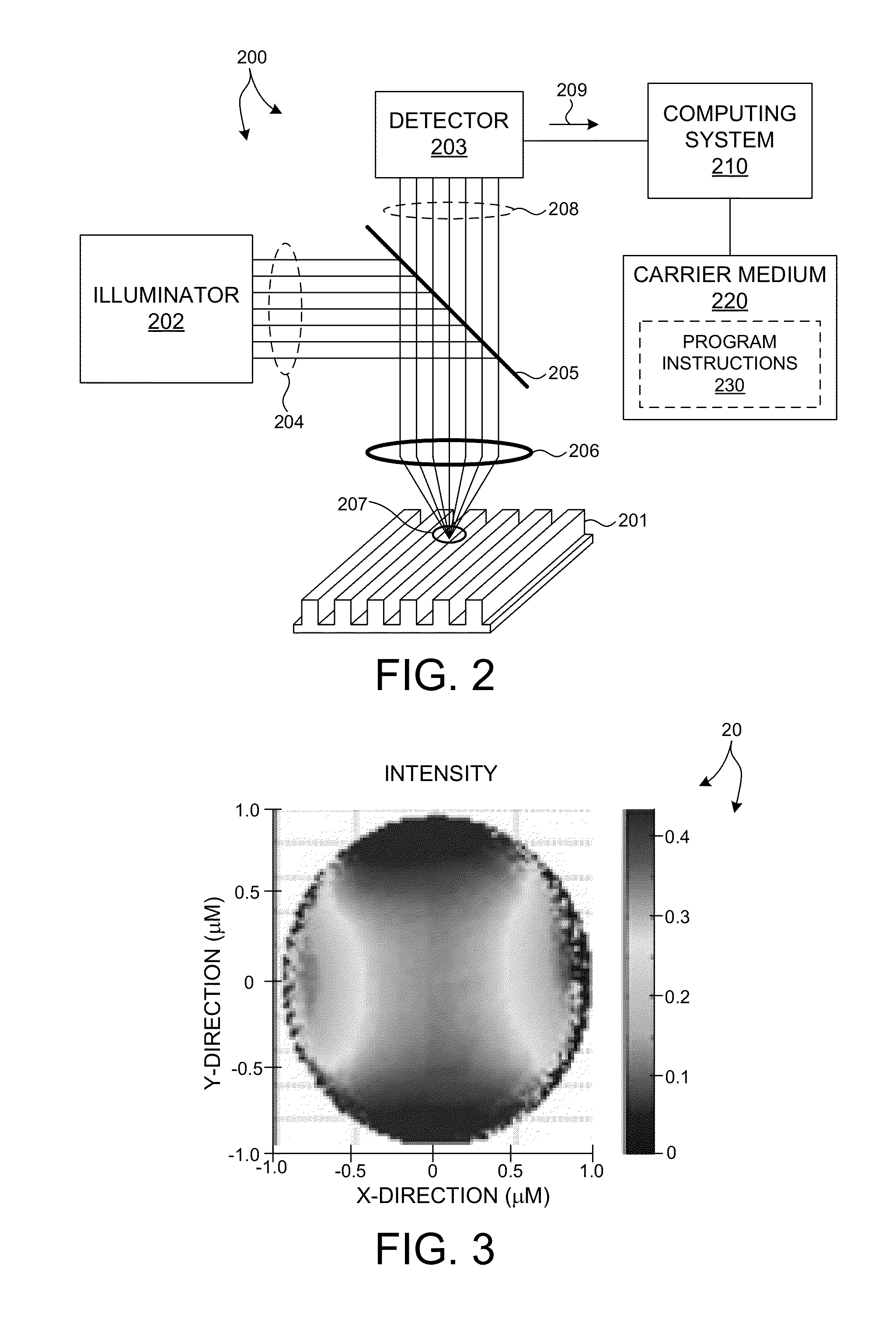
[0036]In an optical metrology or inspection system dedicated to the measurement of nominal structures (e.g., CD metrology, patterned wafer inspection, etc.), detection of a speckle pattern is undesirable measurement noise that degrades the measurement signals indicative of nominal structural parameters (e.g., nominal dimensions and nominal material properties such as lateral critical dimension, feature height, sidewall angle, film thickness, index of refraction, etc). As a consequence, steps are typically taken to reduce the speckle pattern by design (e.g., reduce the degree of spatial coherence of the illumination light) or by data analysis (e.g., averaging signals to remove the effect of the speckle field). However, the inventors have discovered that the speckle field is indicative of important structural irregulari...


PUM


Abstract

Systems and methods are presented to enhance and isolate residual signals indicative of the speckle field based on measurements taken by optically based metrology systems. Structural irregularities such as roughness and topographical errors give rise to light scattered outside of the specularly reflected component of the diffracted light. The scattered light interferes constructively or destructively with the specular component in a high numerical aperture illumination and detection system to form a speckle field. Various methods of determining residual signals indicative of the speckle field are presented. Furthermore, various methods of determining structural irregularities based on analysis of the residual signals are presented. In various embodiments, illumination with a high degree of spatial coherence is provided over any of a wide range of angles of incidence, multiple polarization channels, and multiple wavelength channels. In addition, diffracted light is collected over a wide range of angles of detection.

Description

CROSS REFERENCE TO RELATED APPLICATION[0001]The present application for patent claims priority under 35 U.S.C. §119 from U.S. provisional patent application Ser. No. 61 / 587,593, entitled “Apparatus and Method of Measuring Roughness and Other Parameters of a Structure,” filed Jan. 17, 2012, the subject matter of which is incorporated herein by reference.TECHNICAL FIELD[0002]The described embodiments relate to optical metrology and inspection systems for microscopy, and more particularly to optical metrology and inspection involving speckle analysis.BACKGROUND INFORMATION[0003]Semiconductor devices such as logic and memory devices are typically fabricated by a sequence of processing steps applied to a specimen. The various features and multiple structural levels of the semiconductor devices are formed by these processing steps. For example, lithography among others is one semiconductor fabrication process that involves generating a pattern on a semiconductor wafer. Additional examples...

Claims


Application Information

Patent Timeline
IPC IPC(8): G01B9/02
CPCG01B9/02G01B2210/56G01B11/24
Inventor SHCHEGROV, ANDREI V.BRADY, GREGORYPETERLINZ, KEVIN
Owner KLA TENCOR CORP
Why Eureka
Try Eureka