Structure of electrical contact and fabrication method thereof

a technology of electrical contact and structure, which is applied in the direction of electrical apparatus, semiconductor devices, semiconductor/solid-state device details, etc., can solve the problems of over-consuming thermal budget of semiconductor devices and increase manufacturing costs, and achieve the effect of saving thermal budget of an entire semiconductor device and simplifying the process of fabricating the electrical contact structur

Active Publication Date: 2013-08-01
UNITED MICROELECTRONICS CORP
View PDF7 Cites 19 Cited by
  • Summary
  • Abstract
  • Description
  • Claims
  • Application Information

AI Technical Summary

Benefits of technology

[0010]In sum, the invention provides an electrical contact structure and a fabricating method thereof, which can omit a process for removing the metal layer. In addition, a phase transition process and a process for depositing barrier layer are also combined to other processes. Therefore, processes for fabricating the electrical contact structure may be simplified and thermal budget of an entire semiconductor device may also be saved.

Problems solved by technology

Such complicated steps are no doubt increase cost of the manufacture and the thermal budget of the semiconductor device is over consumed.

Method used


Image

  • Structure of electrical contact and fabrication method thereof
  • Structure of electrical contact and fabrication method thereof
  • Structure of electrical contact and fabrication method thereof

Examples


Embodiment Construction

[0020]In the following description, numerous specific details are given to provide a thorough understanding of the invention. It will, however, be apparent to one skilled in the art that the invention may be practiced without these specific details. Furthermore, some well-known system configurations and process steps are not disclosed in detail, as these should be well-known to those skilled in the art.

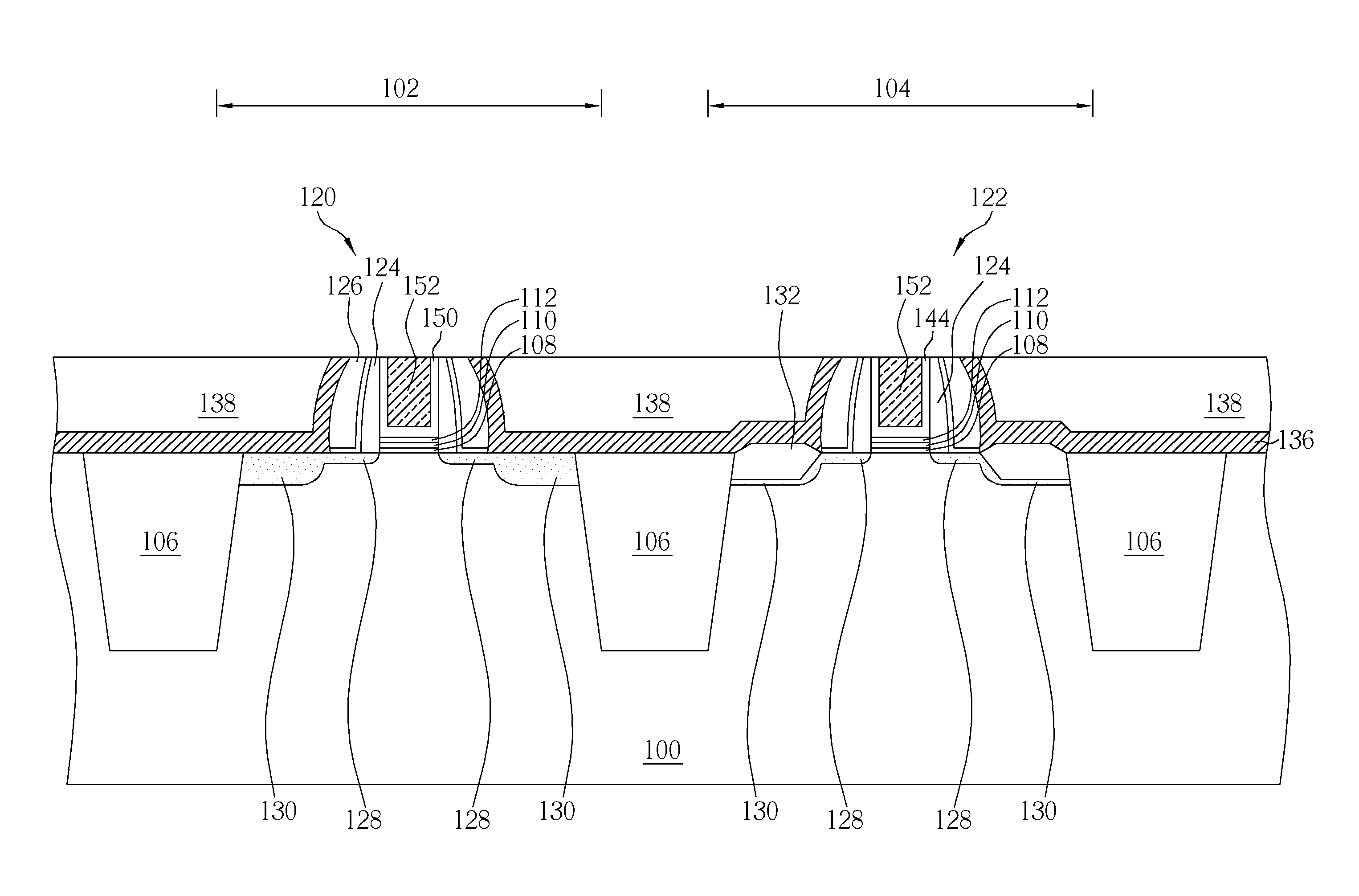
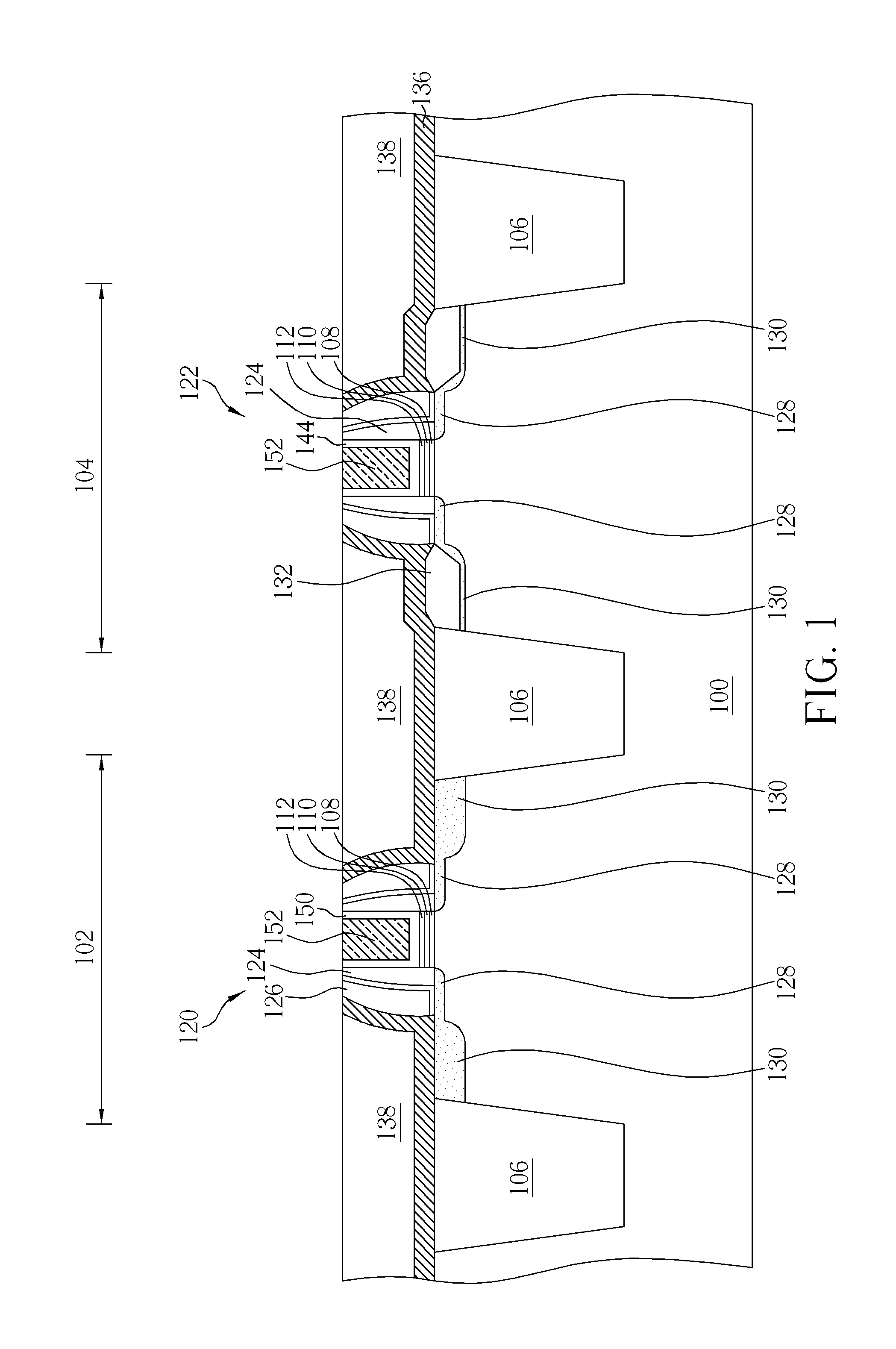
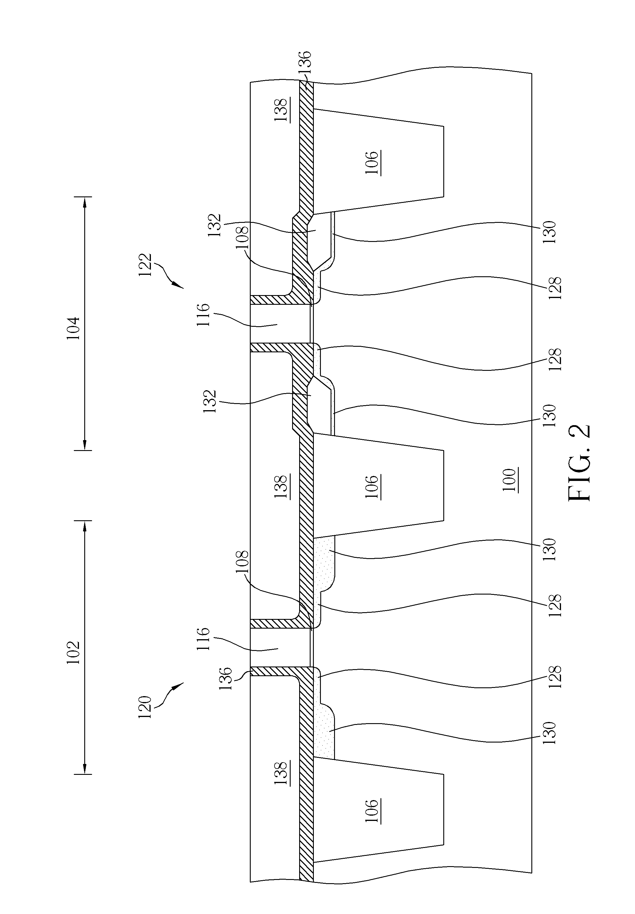
[0021]Please refer to FIGS. 1-10. FIGS. 1-10 are schematic diagrams showing a method for fabricating an electrical contact according to one embodiment of the invention. As shown in FIG. 1, a semiconductor device is provided first, for example, a complementary metal oxide semiconductor transistor (CMOS), which is fabricated through a gate—last process accompanied with a high-k first process. A structure of which is described as follows. A substrate 100, for example, a silicon substrate, a silicon-on-insulator (SOI) or the like is provided. A first region and a second region are defined...


PUM

PropertyMeasurementUnit
temperatureaaaaaaaaaa
thickaaaaaaaaaa
temperatureaaaaaaaaaa

Abstract

A method of fabricating an electrical contact comprises the following steps. A substrate having at least a silicon region is provided. At least an insulation layer is formed on the substrate, wherein the insulation layer comprises at least a contact hole which exposes the silicon region. A metal layer is formed on sidewalls and bottom of the contact hole. An annealing process is performed to form a first metal silicide layer in the silicon region nearby the bottom of the contact hole. A conductive layer covering the metal layer and filling up the contact hole is then formed, wherein the first metal silicide layer is transformed into a second metal silicide layer when the conductive layer is formed.

Description

BACKGROUND OF THE INVENTION[0001]1. Field of the Invention[0002]The present invention generally relates to a structure of an electrical contact. More particularly, the invention relates to an electrical contact connecting semiconductor devices and a fabricating method thereof.[0003]2. Description of the Prior Art[0004]As semiconductor processes advance to very deep sub-micron geometries, such as 20-nm node and beyond, and with the progress of device miniaturization, junction resistance between semiconductors and external contact metals has become a critical issue; therefore, there is a strong need to invent electrical contact structures with relatively low junction resistance, which can be used to connecting semiconductors and conductive lines.[0005]In a convention method of fabricating an electrical contact, in order to reduce junction resistance, a self-aligned silicide (salicide) process is utilized to form a metal silicide layer on the junction of metal and semiconductor layer. ...

Claims


Application Information

Patent Timeline
Patent Type & Authority Applications(United States)
IPC IPC(8): H01L23/532H01L23/522H01L21/768
CPCH01L23/485H01L21/28518H01L21/76843H01L21/76855H01L2924/0002H01L21/823814H01L2924/00H01L23/49866
Inventor TSENG, I-MINGTSAI, TSUNG-LUNGCHEN, YI-WEI
Owner UNITED MICROELECTRONICS CORP
Why Eureka
Try Eureka